CY7C1339G
Electrical Characteristics Over the Operating Range[9, 10] (continued)
Parameter | Description | Test Conditions | Min. | Max. | Unit | |
|
|
|
|
|
|
|
ISB3 | Automatic CE | VDD = Max, Device Deselected, or |
| 105 | mA | |
| VIN ≤ 0.3V or VIN > VDDQ – 0.3V |
|
|
|
| |
|
| 95 | mA | |||
| f = fMAX = 1/tCYC |
|
|
|
| |
|
| 85 | mA | |||
|
|
|
| |||
|
|
|
|
|
|
|
|
|
|
| 75 | mA | |
|
|
|
|
|
|
|
ISB4 | Automatic CE | VDD = Max, Device Deselected, | All Speeds |
| 45 | mA |
| VIN ≥ VIH or VIN ≤ VIL, f = 0 |
|
|
|
| |
|
|
|
|
|
| |
Capacitance[11]
Parameter | Description | Test Conditions | TQFP | BGA | Unit | |
Package | Package | |||||
|
|
|
|
|
| |
CIN | Input Capacitance | TA = 25°C, f = 1 MHz, | 5 | 5 | pF | |
|
| VDD = 3.3V. |
|
|
| |
CCLK | Clock Input Capacitance | 5 | 5 | pF | ||
|
| VDDQ = 3.3V |
|
|
| |
CI/O | Input/Output Capacitance | 5 | 7 | pF | ||
| ||||||
Thermal Resistance[11] |
|
|
|
| ||
Parameter | Description | Test Conditions | TQFP | BGA | Unit | |
Package | Package | |||||
|
|
|
|
|
| |
ΘJA | Thermal Resistance | Test conditions follow standard test | 30.32 | 34.1 | °C/W | |
| (Junction to Ambient) | methods and procedures for |
|
|
| |
|
| measuring thermal impedance, per |
|
|
| |
ΘJC | Thermal Resistance | 6.85 | 14.0 | °C/W | ||
EIA/JESD51 | ||||||
| (Junction to Case) |
|
|
|
|
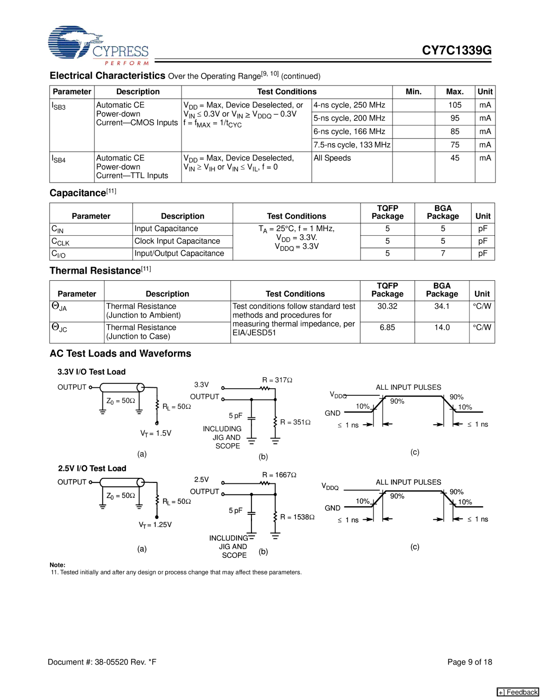
AC Test Loads and Waveforms
3.3V I/O Test Load
OUTPUT |
|
|
|
|
|
|
|
|
|
|
|
|
| 3.3V |
|
|
|
|
|
|
| R = 317Ω |
|
|
|
|
| ALL INPUT PULSES | ||||||||||||||||
|
|
|
|
|
|
|
|
|
|
|
|
|
|
|
|
|
|
|
|
|
|
|
|
|
|
|
| VDDQ |
|
|
|
| ||||||||||||
|
|
|
|
|
| Z0 | = 50Ω |
|
|
|
| OUTPUT |
|
|
|
|
|
|
|
|
|
|
|
|
|
|
|
|
|
|
|
|
|
|
|
|
|
| ||||||
|
|
|
|
|
|
| RL | = 50Ω |
|
|
|
|
|
|
|
|
|
|
|
|
|
|
| 10% |
|
|
|
|
|
| 90% |
|
| |||||||||||
|
|
|
|
|
|
|
|
|
|
|
|
|
|
|
|
|
|
|
|
|
|
|
|
|
|
|
|
|
|
|
|
|
|
|
|
|
| |||||||
|
|
|
|
|
|
|
|
|
|
|
|
|
|
| 5 pF |
|
|
|
|
|
|
|
|
|
|
|
|
| R = 351Ω | GND |
|
|
|
|
|
|
|
|
|
|
| |||
|
|
|
|
|
|
|
|
|
|
|
|
|
|
|
|
|
|
|
|
|
|
|
|
|
|
|
|
|
|
|
|
|
|
|
|
| ||||||||
|
|
|
|
|
|
|
|
|
|
|
|
|
| INCLUDING |
|
|
|
|
|
|
|
|
|
|
|
|
| ≤ 1 ns |
|
|
|
|
|
|
|
|
| |||||||
|
|
|
|
|
|
|
|
|
| VT = 1.5V |
|
|
|
|
|
|
|
|
|
|
|
|
|
|
|
|
|
|
|
|
|
| ||||||||||||
|
|
|
|
|
|
|
|
|
|
|
|
|
|
|
|
|
|
|
|
|
|
|
|
|
|
|
|
|
|
|
|
|
| |||||||||||
|
|
|
|
|
|
|
|
|
|
|
|
|
|
|
|
|
|
|
|
|
|
|
|
|
|
|
|
|
|
|
|
|
|
|
|
|
| |||||||
|
|
|
|
|
|
|
|
|
| JIG AND |
|
|
|
|
|
|
|
|
|
|
|
|
|
|
|
|
|
|
|
|
|
|
|
|
|
|
|
|
| |||||
|
|
|
|
|
|
|
|
|
|
|
|
|
|
|
|
|
|
|
|
|
|
|
|
|
|
|
|
|
|
|
|
|
|
|
| |||||||||
|
|
|
|
|
|
|
|
| (a) | SCOPE |
|
|
|
|
|
|
|
|
|
|
|
|
|
|
|
|
|
|
|
|
|
|
|
|
| (c) | ||||||||
|
|
|
|
|
|
|
|
|
|
|
|
|
| (b) |
|
|
|
|
|
|
|
|
|
| ||||||||||||||||||||
|
|
|
|
|
|
|
|
|
|
|
|
|
|
|
|
|
|
|
|
|
|
|
|
|
|
| ||||||||||||||||||
|
|
|
|
|
|
|
|
|
|
|
|
|
|
|
|
|
|
|
|
|
|
|
|
|
|
|
|
|
|
|
|
|
|
| ||||||||||
2.5V I/O Test Load |
|
|
|
|
|
|
|
|
| R = 1667Ω |
|
|
|
|
|
|
|
|
|
|
|
|
| |||||||||||||||||||||
OUTPUT |
|
|
|
|
|
|
|
|
|
|
|
|
| 2.5V |
|
|
|
|
|
|
|
|
|
|
|
| ALL INPUT PULSES | |||||||||||||||||
|
|
|
|
|
|
|
|
|
|
|
|
|
|
|
|
|
|
|
|
|
|
|
|
|
|
|
| VDDQ |
|
|
|
| ||||||||||||
|
|
|
|
|
| Z0 | = 50Ω |
|
|
|
| OUTPUT |
|
|
|
|
|
|
|
|
|
|
|
|
|
|
|
|
|
|
|
|
|
|
|
|
|
| ||||||
|
|
|
|
|
|
| RL | = 50Ω |
|
|
|
|
|
|
|
|
|
|
|
|
|
|
| 10% |
|
|
| 90% |
|
| ||||||||||||||
|
|
|
|
|
|
|
|
|
|
|
|
|
|
|
|
|
|
|
|
|
|
|
|
|
|
|
|
|
|
|
|
|
|
|
|
|
| |||||||
|
|
|
|
|
|
|
|
|
|
|
|
|
|
| 5 pF |
|
|
|
|
|
|
|
|
|
|
|
|
| R = 1538Ω | GND |
|
|
|
|
|
|
|
|
|
| ||||
|
|
|
|
|
|
|
|
|
|
|
|
|
|
|
|
|
|
|
|
|
|
|
|
|
|
|
|
|
|
|
|
|
|
|
|
| ||||||||
|
|
|
|
|
|
|
|
|
|
|
|
|
|
|
|
|
|
|
|
|
|
|
|
|
|
|
|
|
| ≤ 1 ns |
|
|
|
|
|
|
|
|
| |||||
|
|
|
|
|
|
|
|
|
|
|
|
|
|
|
|
|
|
|
|
|
|
|
|
|
|
|
|
|
|
|
|
|
|
|
|
|
|
| ||||||
|
|
|
|
|
|
|
|
|
| VT = 1.25V |
|
|
|
|
|
|
|
|
|
|
|
|
|
|
|
|
|
|
|
|
|
|
| |||||||||||
|
|
|
|
|
|
|
|
|
|
|
|
|
|
|
|
|
|
|
|
|
|
|
|
|
|
|
|
|
|
|
|
|
| |||||||||||
|
|
|
|
|
|
|
|
|
|
|
|
|
|
|
|
|
|
|
|
|
|
|
|
|
|
|
|
|
|
|
|
|
|
|
|
|
| |||||||
90%
10%
≤ 1 ns
90%
10%
≤ 1 ns
| INCLUDING |
|
|
|
|
|
|
| (c) |
|
|
|
|
|
|
|
| ||
|
|
|
|
|
|
|
| ||
(a) | JIG AND |
|
|
| (b) |
|
|
| |
| SCOPE |
|
|
|
|
|
|
| |
|
|
|
|
|
|
|
|
|
Note:
11. Tested initially and after any design or process change that may affect these parameters.
Document #: | Page 9 of 18 |
[+] Feedback