CY7C1339G
signal. Consecutive single Read cycles are supported. Once the SRAM is deselected at clock rise by the chip select and either ADSP or ADSC signals, its output will
Single Write Accesses Initiated by ADSP
This access is initiated when both of the following conditions are satisfied at clock rise: (1) ADSP is asserted LOW, and
(2)CE1, CE2, CE3 are all asserted active. The address presented to A is loaded into the address register and the address advancement logic while being delivered to the
memory array. The Write signals (GW, BWE, and BW[A:D]) and ADV inputs are ignored during this first cycle.
Because the CY7C1339G is a common I/O device, the Output Enable (OE) must be deserted HIGH before presenting data to the DQs inputs. Doing so will
Single Write Accesses Initiated by ADSC
ADSC Write accesses are initiated when the following condi- tions are satisfied: (1) ADSC is asserted LOW, (2) ADSP is deserted HIGH, (3) CE1, CE2, CE3 are all asserted active, and
(4) the appropriate combination of the Write inputs (GW, BWE, and BW[A:D]) are asserted active to conduct a Write to the desired byte(s).
Because the CY7C1339G is a common I/O device, the Output Enable (OE) must be deserted HIGH before presenting data
to the DQs inputs. Doing so will
Burst Sequences
The CY7C1339G provides a
Asserting ADV LOW at clock rise will automatically increment the burst counter to the next address in the burst sequence. Both Read and Write burst operations are supported.
Sleep Mode
The ZZ input pin is an asynchronous input. Asserting ZZ places the SRAM in a power conservation “sleep” mode. Two clock cycles are required to enter into or exit from this “sleep” mode. While in this mode, data integrity is guaranteed. Accesses pending when entering the “sleep” mode are not considered valid nor is the completion of the operation guaranteed. The device must be deselected prior to entering the “sleep” mode. CE1, CE2, CE3, ADSP, and ADSC must remain inactive for the duration of tZZREC after the ZZ input returns LOW.
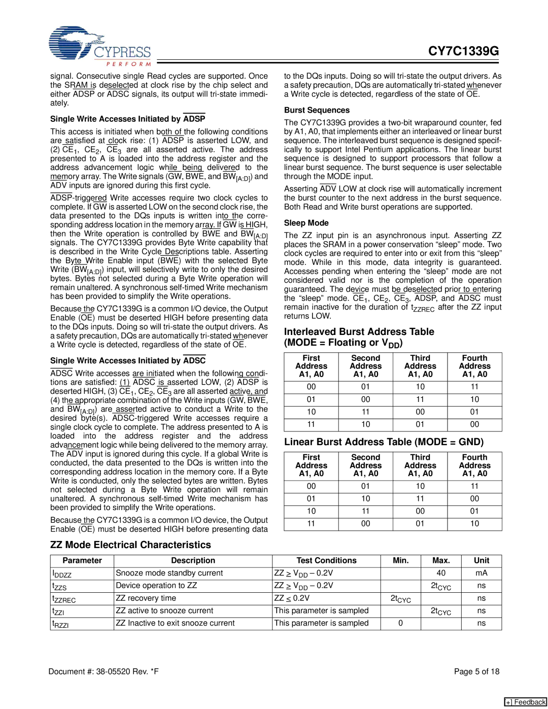
Interleaved Burst Address Table (MODE = Floating or VDD)
First | Second | Third | Fourth |
Address | Address | Address | Address |
A1, A0 | A1, A0 | A1, A0 | A1, A0 |
00 | 01 | 10 | 11 |
|
|
|
|
01 | 00 | 11 | 10 |
|
|
|
|
10 | 11 | 00 | 01 |
|
|
|
|
11 | 10 | 01 | 00 |
|
|
|
|
Linear Burst Address Table (MODE = GND)
First | Second | Third | Fourth |
Address | Address | Address | Address |
A1, A0 | A1, A0 | A1, A0 | A1, A0 |
00 | 01 | 10 | 11 |
|
|
|
|
01 | 10 | 11 | 00 |
|
|
|
|
10 | 11 | 00 | 01 |
|
|
|
|
11 | 00 | 01 | 10 |
|
|
|
|
ZZ Mode Electrical Characteristics
Parameter | Description | Test Conditions | Min. | Max. | Unit |
IDDZZ | Snooze mode standby current | ZZ > VDD – 0.2V |
| 40 | mA |
tZZS | Device operation to ZZ | ZZ > VDD – 0.2V |
| 2tCYC | ns |
tZZREC | ZZ recovery time | ZZ < 0.2V | 2tCYC |
| ns |
tZZI | ZZ active to snooze current | This parameter is sampled |
| 2tCYC | ns |
tRZZI | ZZ Inactive to exit snooze current | This parameter is sampled | 0 |
| ns |
Document #: | Page 5 of 18 |
[+] Feedback