CY7C1355C
CY7C1357C
precaution, DQs and DQPX are automatically
Burst Write Accesses
The CY7C1355C/CY7C1357C has an
Sleep Mode
The ZZ input pin is an asynchronous input. Asserting ZZ places the SRAM in a power conservation “sleep” mode. Two clock cycles are required to enter into or exit from this “sleep” mode. While in this mode, data integrity is guaranteed. Accesses pending when entering the “sleep” mode are not considered valid nor is the completion of the operation guaranteed. The device must be deselected prior to entering the “sleep” mode. CE1, CE2, and CE3, must remain inactive for the duration of tZZREC after the ZZ input returns LOW.
. .
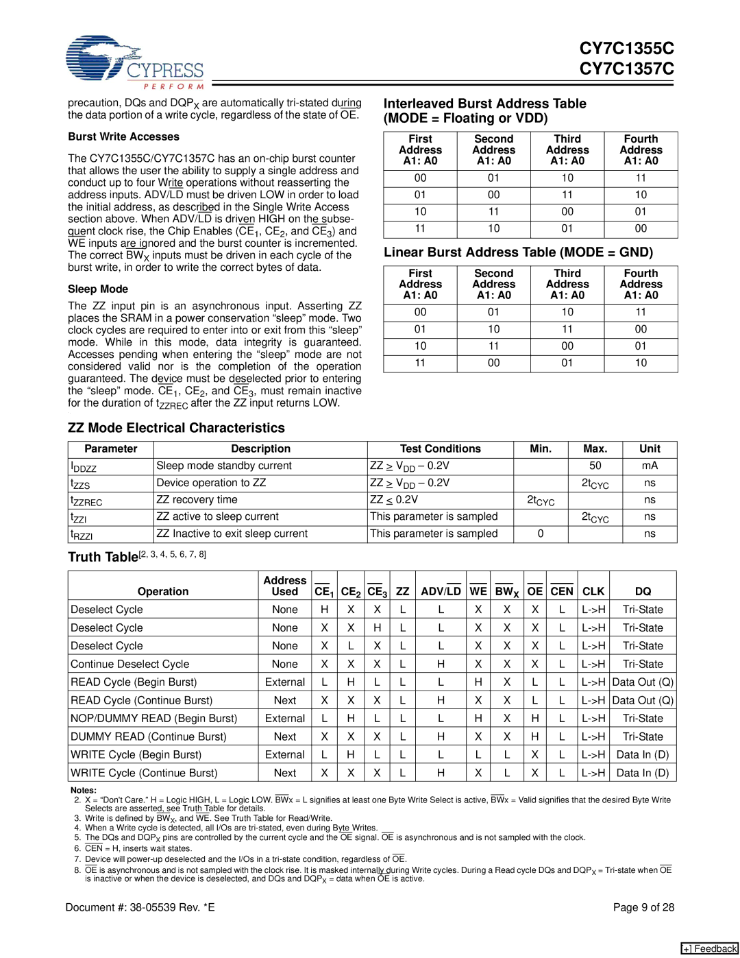
Interleaved Burst Address Table (MODE = Floating or VDD)
First | Second | Third | Fourth |
Address | Address | Address | Address |
A1: A0 | A1: A0 | A1: A0 | A1: A0 |
00 | 01 | 10 | 11 |
|
|
|
|
01 | 00 | 11 | 10 |
|
|
|
|
10 | 11 | 00 | 01 |
|
|
|
|
11 | 10 | 01 | 00 |
|
|
|
|
Linear Burst Address Table (MODE = GND)
First | Second | Third | Fourth |
Address | Address | Address | Address |
A1: A0 | A1: A0 | A1: A0 | A1: A0 |
00 | 01 | 10 | 11 |
|
|
|
|
01 | 10 | 11 | 00 |
|
|
|
|
10 | 11 | 00 | 01 |
|
|
|
|
11 | 00 | 01 | 10 |
|
|
|
|
ZZ Mode Electrical Characteristics
Parameter | Description |
|
|
|
|
|
| Test Conditions |
|
|
|
|
| Min. |
|
|
| Max. |
| Unit | |||||||||||
IDDZZ | Sleep mode standby current |
|
|
|
| ZZ > VDD – 0.2V |
|
|
|
|
|
|
|
|
|
|
|
|
|
| 50 |
| mA | ||||||||
tZZS | Device operation to ZZ |
|
|
|
| ZZ > VDD – 0.2V |
|
|
|
|
|
|
|
|
|
|
|
|
|
|
| 2tCYC |
| ns | |||||||
tZZREC | ZZ recovery time |
|
|
|
|
|
| ZZ < 0.2V |
|
|
|
|
|
|
|
|
|
| 2tCYC |
|
|
|
|
| ns | ||||||
tZZI | ZZ active to sleep current |
|
|
|
| This parameter is sampled |
|
|
|
|
|
|
|
|
| 2tCYC |
| ns | |||||||||||||
tRZZI | ZZ Inactive to exit sleep current |
|
|
|
| This parameter is sampled |
|
| 0 |
|
|
|
|
|
|
| ns | ||||||||||||||
Truth Table[2, 3, 4, 5, 6, 7, 8] |
|
|
|
|
|
|
|
|
|
|
|
|
|
|
|
|
|
|
|
|
|
|
|
|
|
|
|
|
|
| |
|
| Address |
|
|
|
|
|
|
|
|
|
|
|
|
|
|
|
|
|
|
|
|
|
|
|
|
|
|
|
|
|
Operation | Used |
| CE | 1 | CE2 |
| CE | 3 | ZZ |
| ADV/LD |
|
| WE |
|
| BWX |
| OE | CEN |
| CLK |
| DQ | |||||||
Deselect Cycle |
| None |
| H | X |
| X | L |
| L |
|
| X |
|
| X |
| X |
|
| L |
|
| ||||||||
Deselect Cycle |
| None |
| X | X |
| H | L |
| L |
|
| X |
|
| X |
| X |
|
| L |
|
| ||||||||
Deselect Cycle |
| None |
| X | L |
| X | L |
| L |
|
| X |
|
| X |
| X |
|
| L |
|
| ||||||||
Continue Deselect Cycle | None |
| X | X |
| X | L |
| H |
|
| X |
|
| X |
| X |
|
| L |
|
| |||||||||
READ Cycle (Begin Burst) | External |
| L | H |
| L | L |
| L |
|
| H |
|
| X |
| L |
|
| L |
| Data Out (Q) | |||||||||
READ Cycle (Continue Burst) | Next |
| X | X |
| X | L |
| H |
|
| X |
|
| X |
| L |
|
| L |
| Data Out (Q) | |||||||||
NOP/DUMMY READ (Begin Burst) | External |
| L | H |
| L | L |
| L |
|
| H |
|
| X |
| H |
|
| L |
|
| |||||||||
DUMMY READ (Continue Burst) | Next |
| X | X |
| X | L |
| H |
|
| X |
|
| X |
| H |
|
| L |
|
| |||||||||
WRITE Cycle (Begin Burst) | External |
| L | H |
| L | L |
| L |
|
| L |
|
| L |
| X |
|
| L |
| Data In (D) | |||||||||
WRITE Cycle (Continue Burst) | Next |
| X | X |
| X | L |
| H |
|
| X |
|
| L |
| X |
|
| L |
| Data In (D) | |||||||||
Notes:
2.X = “Don't Care.” H = Logic HIGH, L = Logic LOW. BWx = L signifies at least one Byte Write Select is active, BWx = Valid signifies that the desired Byte Write Selects are asserted, see Truth Table for details.
3.Write is defined by BWX, and WE. See Truth Table for Read/Write.
4.When a Write cycle is detected, all I/Os are
5.The DQs and DQPX pins are controlled by the current cycle and the OE signal. OE is asynchronous and is not sampled with the clock.
6.CEN = H, inserts wait states.
7.Device will
8.OE is asynchronous and is not sampled with the clock rise. It is masked internally during Write cycles. During a Read cycle DQs and DQPX =
Document #: | Page 9 of 28 |
[+] Feedback