CY7C1480V25
CY7C1482V25
CY7C1486V25
DQs are automatically
Single Write Accesses Initiated by ADSC
ADSC Write accesses are initiated when the following condi- tions are satisfied: (1) ADSC is asserted LOW, (2) ADSP is deasserted HIGH, (3) CE1, CE2, CE3 are all asserted active, and (4) the appropriate combination of the write inputs (GW, BWE, and BWX) are asserted active to conduct a write to the desired byte(s).
Because CY7C1480V25/CY7C1482V25/CY7C1486V25 is a common IO device, the Output Enable (OE) must be deasserted HIGH before presenting data to the DQs inputs. Doing so
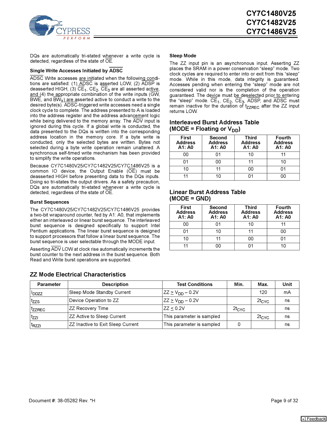
Burst Sequences
The CY7C1480V25/CY7C1482V25/CY7C1486V25 provides a
Asserting ADV LOW at clock rise automatically increments the burst counter to the next address in the burst sequence. Both Read and Write burst operations are supported.
Sleep Mode
The ZZ input pin is an asynchronous input. Asserting ZZ places the SRAM in a power conservation “sleep” mode. Two clock cycles are required to enter into or exit from this “sleep” mode. While in this mode, data integrity is guaranteed. Accesses pending when entering the “sleep” mode are not considered valid nor is the completion of the operation guaranteed. The device must be deselected prior to entering the “sleep” mode. CE1, CE2, CE3, ADSP, and ADSC must remain inactive for the duration of tZZREC after the ZZ input returns LOW.
Interleaved Burst Address Table (MODE = Floating or VDD)
First | Second | Third | Fourth |
Address | Address | Address | Address |
A1: A0 | A1: A0 | A1: A0 | A1: A0 |
00 | 01 | 10 | 11 |
01 | 00 | 11 | 10 |
10 | 11 | 00 | 01 |
11 | 10 | 01 | 00 |
Linear Burst Address Table (MODE = GND)
First | Second | Third | Fourth |
Address | Address | Address | Address |
A1: A0 | A1: A0 | A1: A0 | A1: A0 |
00 | 01 | 10 | 11 |
01 | 10 | 11 | 00 |
10 | 11 | 00 | 01 |
11 | 00 | 01 | 10 |
ZZ Mode Electrical Characteristics
Parameter | Description | Test Conditions | Min. | Max. | Unit |
|
|
|
|
|
|
IDDZZ | Sleep Mode Standby Current | ZZ > VDD – 0.2V |
| 120 | mA |
tZZS | Device Operation to ZZ | ZZ > VDD – 0.2V |
| 2tCYC | ns |
tZZREC | ZZ Recovery Time | ZZ < 0.2V | 2tCYC |
| ns |
tZZI | ZZ Active to Sleep Current | This parameter is sampled |
| 2tCYC | ns |
tRZZI | ZZ Inactive to Exit Sleep Current | This parameter is sampled | 0 |
| ns |
Document #: | Page 9 of 32 |
[+] Feedback