CY7C1480V25
CY7C1482V25
CY7C1486V25
IEEE 1149.1 Serial Boundary Scan (JTAG)
The CY7C1480V25/CY7C1482V25/CY7C1486V25 incorpo- rates a serial boundary scan test access port (TAP). This port operates in accordance with IEEE Standard
The CY7C1480V25/CY7C1482V25/CY7C1486V25 contains a TAP controller, instruction register, boundary scan register, bypass register, and ID register.
Disabling the JTAG Feature
Test Mode Select (TMS)
The TMS input gives commands to the TAP controller and is sampled on the rising edge of TCK. You can leave this ball unconnected if the TAP is not used. The ball is pulled up inter- nally, resulting in a logic HIGH level.
Test Data-In (TDI)
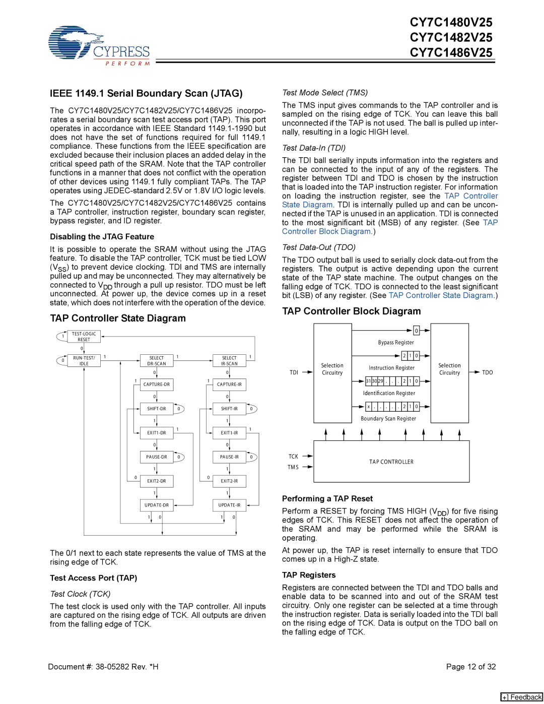
The TDI ball serially inputs information into the registers and can be connected to the input of any of the registers. The register between TDI and TDO is chosen by the instruction that is loaded into the TAP instruction register. For information on loading the instruction register, see the TAP Controller State Diagram. TDI is internally pulled up and can be uncon- nected if the TAP is unused in an application. TDI is connected to the most significant bit (MSB) of any register. (See TAP Controller Block Diagram.)
It is possible to operate the SRAM without using the JTAG feature. To disable the TAP controller, TCK must be tied LOW (VSS) to prevent device clocking. TDI and TMS are internally pulled up and may be unconnected. They may alternatively be connected to VDD through a pull up resistor. TDO must be left unconnected. At power up, the device comes up in a reset state, which does not interfere with the operation of the device.
TAP Controller State Diagram
Test Data-Out (TDO)
The TDO output ball is used to serially clock
TAP Controller Block Diagram
1![]()
0
0![]()
IDLE
SELECT | 1 | SELECT | 1 |
|
| ||
0 |
| 0 |
|
1 |
| 1 |
|
CA |
| CA |
|
0 |
| 0 |
|
0 | 0 | ||
1 |
| 1 |
|
1 | 1 | ||
|
| ||
0 |
| 0 |
|
TDI
Selection Circuitry
|
|
|
|
|
|
|
|
|
| 0 |
|
|
|
|
|
|
|
|
|
|
|
| |
|
|
| Bypass Register |
|
| ||||||
|
|
|
|
|
|
|
|
|
|
|
|
|
|
|
|
|
|
|
| 2 | 1 | 0 |
|
|
|
|
|
|
|
|
|
| |||
|
|
|
|
|
|
|
|
|
|
|
|
| Instruction Register |
|
| ||||||||
|
|
|
|
|
|
|
|
|
|
|
|
| 31 | 30 | 29 | . | . | . | 2 | 1 | 0 |
| |
|
| ||||||||||
|
|
|
|
|
|
|
|
|
|
|
|
Identification Register |
| ||||||||||
|
|
|
|
|
|
|
|
| |||
| x | . | . | . | . | . | 2 | 1 | 0 |
| |
|
| ||||||||||
|
|
|
|
|
|
|
|
|
|
|
|
Boundary Scan Register
Selection Circuitry
TDO
|
| PA | 0 |
|
| PA | 0 | |||||||
|
|
|
|
|
|
|
|
|
|
|
|
|
|
|
|
|
| 1 |
|
|
|
|
|
| 1 |
|
|
|
|
0 |
|
|
|
|
|
| 0 |
|
|
|
|
|
| |
|
|
|
| |||||||||||
|
|
|
|
|
|
| ||||||||
|
|
|
|
|
|
| ||||||||
|
|
|
|
|
|
|
|
|
|
|
|
|
|
|
|
|
| 1 |
|
|
|
|
|
| 1 |
|
|
|
|
|
|
|
|
|
|
|
|
|
|
|
|
|
|
|
|
| UPDA |
|
|
| UPDA |
|
| ||||||
|
|
|
|
|
|
| ||||||||
|
|
|
|
|
|
|
|
|
|
|
|
|
|
|
1 | 0 |
|
|
| 1 | 0 |
|
|
| |||||
|
|
|
|
|
|
|
|
|
|
|
|
|
|
|
|
|
|
|
|
|
|
|
|
|
|
|
|
|
|
TCK
TAP CONTROLLER
TM S
Performing a TAP Reset
Perform a RESET by forcing TMS HIGH (VDD) for five rising edges of TCK. This RESET does not affect the operation of the SRAM and may be performed while the SRAM is operating.
The 0/1 next to each state represents the value of TMS at the rising edge of TCK.
Test Access Port (TAP)
Test Clock (TCK)
The test clock is used only with the TAP controller. All inputs are captured on the rising edge of TCK. All outputs are driven from the falling edge of TCK.
At power up, the TAP is reset internally to ensure that TDO comes up in a
TAP Registers
Registers are connected between the TDI and TDO balls and enable data to be scanned into and out of the SRAM test circuitry. Only one register can be selected at a time through the instruction register. Data is serially loaded into the TDI ball on the rising edge of TCK. Data is output on the TDO ball on the falling edge of TCK.
Document #: | Page 12 of 32 |
[+] Feedback