CY7C1516KV18, CY7C1520KV18, CY7C1527KV18, CY7C1518KV18 specifications
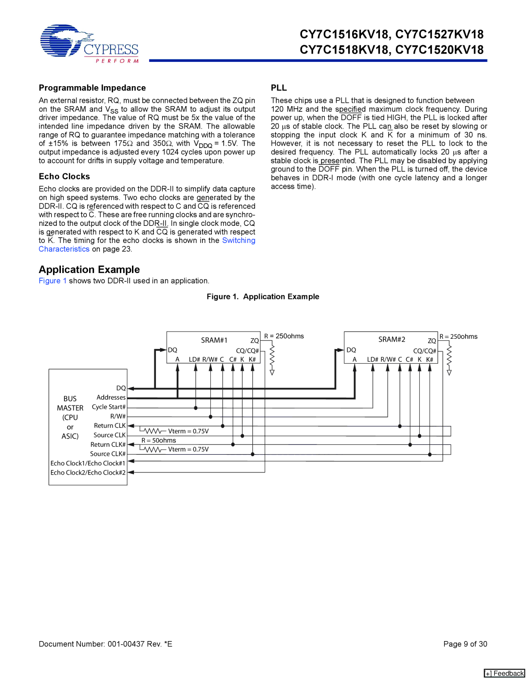
The Cypress CY7C1516KV18, CY7C1520KV18, CY7C1527KV18, and CY7C1518KV18 are a series of high-performance asynchronous static random-access memory (SRAM) devices designed for a variety of applications requiring fast data access and reliable operation. These SRAM chips feature density options ranging from 1Mbit to 4Mbit, catering to a broad spectrum of consumer electronics, telecommunications, networking, and industrial applications.One of the standout features of these devices is their high-speed access times, which typically range from 12 ns to 15 ns, allowing for rapid data retrieval and writing. This speed makes them ideal for applications where low latency is crucial, such as in cache memory systems and high-speed computing. The low power consumption of these devices also makes them attractive for battery-operated equipment, as they can operate effectively while minimizing energy usage.
The CY7C1516KV18 and other models in this series incorporate advanced CMOS technology, which is instrumental in achieving low standby and active power requirements. This technology not only enhances the overall efficiency of the memory devices but also contributes to reduced thermal generation, which is an essential factor in maintaining performance and longevity in high-density applications.
Data integrity is another critical characteristic of these SRAM devices. They are designed with features such as byte-write capability and asynchronous read/write operations, ensuring that users can manage data efficiently and reliably. The robust architecture also allows for simple interfacing with most processors and microcontrollers, facilitating easy integration into various systems.
The packages of these SRAM chips are available in several form factors, including 44-pin and 48-pin configurations, allowing for flexibility in board design and layout. Their compatibility with standard interface protocols ensures seamless communication with other components of electronic designs.
These Cypress SRAM devices support a range of temperature specifications, making them suitable for both commercial and industrial-grade applications. Enhanced reliability during various operating conditions assures designers that these memory chips will maintain performance in diverse environments.
In summary, the Cypress CY7C1516KV18, CY7C1520KV18, CY7C1527KV18, and CY7C1518KV18 SRAM devices offer high speed, low power consumption, and flexibility in integration. With their advanced technology and robust features, these memory solutions continue to play a vital role in modern electronics, driving innovation across multiple sectors.

