1. Features
2. Logic Block Diagram
CY7C601xx, CY7C602xx
Cypress Semiconductor Corporation
5. Conventions
3. Applications
4. Introduction
Figure 6-1. Package Configurations Top View
6. Pinouts
CY7C60223
24-Pin PDIP
CY7C601xx, CY7C602xx
6.1 Pin Assignments
Table 6-1. Pin Assignments
Name
Table 6-1. Pin Assignments continued
Default
7. Register Summary
Table 7-1. enCoRe II LV Register Summary
Addr
Table 7-1. enCoRe II LV Register Summary continued
8. CPU Architecture
9. CPU Registers
9.1 Flags Register
Table 8-1. CPU Registers and Register Name
9.1.1 Accumulator Register
Table 9-2. CPU Accumulator Register CPUA
9.1.2 Index Register
Table 9-3. CPU X Register CPUX
9.2 Addressing Modes
9.2.1 Source Immediate
Table 9-7. Source Immediate
Opcode
9.2.5 Destination Indexed
Table 9-11. Destination Indexed
Example
9.2.6 Destination Direct Source Immediate
10. Instruction Set Summary
9.2.9 Source Indirect Post Increment
Table 9-15. Source Indirect Post Increment
9.2.10 Destination Indirect Post Increment
CY7C601xx, CY7C602xx
11. Memory Organization
11.1 Flash Program Memory Organization
Figure 11-1. Program Memory Space with Interrupt Vector Table
0x1FFF
11.2 Data Memory Organization
11.3 Flash
11.4 SROM
Figure 11-2. Data Memory Organization
11.5.1 SWBootReset Function
11.5 SROM Function Descriptions
Table 11-2. SROM Function Parameters
Variable Name
Settings
11.5.3 WriteBlock Function
Table 11-5. WriteBlock Parameters
11.5.4 EraseBlock Function
Table 11-8. ProtectBlock Parameters
11.5.6 EraseAll Function
11.5.7 TableRead Function
Table 11-10. Table Read Parameters
11.6 SROM Table Read Description
Page 19 of
eg ti
Table 12-1. Oscillator Trim Values vs. Voltage Settings
12. Clocking
12.1 Trim Values for the IOSCTR Register
Gain value for the register at location 0x38 3.3V =
12.2 Clock Architecture Description
12.2.1 CPU Clock
Figure 12-1. CPU Clock Block Diagram
Table 12-2. CPU Clock Configuration CPUCLKCR 0x30 R/W
Bit 71 Reserved
Table 12-3. OSC Control 0 OSCCR0 0x1E0 R/W
Sleep Timer
Sleep Timer Clock
CPU when Internal
Table 12-3. OSC Control 0 OSCCR0 0x1E0 R/W continued
Bit 75 Reserved
Table 12-4. Clock IO Configuration CLKIOCR 0x32 R/W
12.2.2 Interval Timer Clock ITMRCLK
Figure 12-3. Timer Capture Block Diagram
Figure 12-2. Programmable Interval Timer Block Diagram
12.2.3 Timer Capture Clock TCAPCLK
Table 12-5. Timer Clock Configuration TMRCLKCR 0x31 R/W
Page 27 of
XGM Setting
12.2.4 Internal Clock Trim
Table 12-6. IOSC Trim IOSCTR 0x34 R/W
Bit 40 Gain
Table 12-8. LPOSC Trim LPOSCTR 0x36 R/W
12.3 CPU Clock During Sleep Mode
12.2.6 LPOSC Trim
13. Reset
Table 13-1. System Status and Control Register CPUSCR 0xFF R/W
Bit 7 GIES
Bit 5 WDRS
13.1 Power On Reset
13.2 Watchdog Timer Reset
Table 13-2. Reset Watchdog Timer RESWDT 0xE3 W
14. Sleep Mode
14.1.1 Low Power in Sleep Mode
14.1 Sleep Sequence
CPUCLK IOW SLEEP BRQ BRA PD
Figure 14-1. Sleep Timing
14.2 Wakeup Sequence
Figure 14-2. Wakeup Timing
15. Low Voltage Detect Control
Table 15-1. Low Voltage Control Register LVDCR 0x1E3 R/W
Bit 76 Reserved Bit 54 PORLEV10
Bit 20 VM20
15.1 POR Compare State
15.2 ECO Trim Register
Table 15-2. Voltage Monitor Comparators Register VLTCMP 0x1E4 R
Bit 72 Reserved Bit 1 LVD
16. General Purpose IO Ports
16.1 Port Data Registers
16.1.1 P0 Data
Table 16-1. P0 Data Register P0DATA0x00 R/W
16.2 GPIO Port Configuration
16.2.1 Int Enable
16.1.3 P2 Data
Table 16-3. P2 Data Register P2DATA 0x02 R/W
16.2.7 Output Enable
16.2.6 Pull Up Enable
Figure 16-1. GPIO Block Diagram
16.2.9 P0.0/CLKIN Configuration
16.2.11 P0.2/INT0-P0.4/INT2 Configuration
16.2.10 P0.1/CLKOUT Configuration
Table 16-7. P0.1/CLKOUT Configuration P01CR 0x06 R/W
16.2.12 P0.5/TIO0-P0.6/TIO1 Configuration
16.2.13 P0.7 Configuration
Table 16-10. P0.7 Configuration P07CR 0x0C R/W
16.2.14 P1.0 Configuration
16.2.15 P1.1 Configuration
Table 16-12. P1.1 Configuration P11CR 0x0E R/W
16.2.16 P1.2 Configuration
Table 16-13. P1.2 Configuration P12CR 0x0F R/W
16.2.18 P1.4-P1.6 Configuration SCLK, SMOSI, SMISO
Table 16-15. P1.4-P1.6 Configuration P14CR-P16CR 0x11-0x13 R/W
16.2.19 P1.7 Configuration
Table 16-16. P1.7 Configuration P17CR 0x14 R/W
16.2.21 P3 Configuration
Table 16-18. P3 Configuration P3CR 0x16 R/W
16.2.22 P4 Configuration
Table 16-19. P4 Configuration P4CR 0x17 R/W
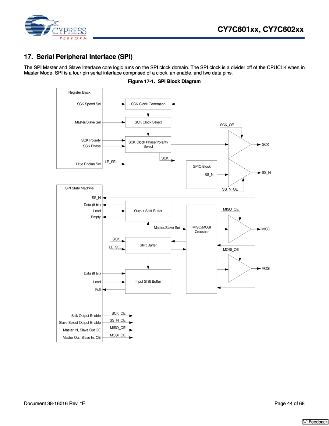
Figure 17-1. SPI Block Diagram
17. Serial Peripheral Interface SPI
17.2 SPI Configure Register
Table 17-2. SPI Configure Register SPICR 0x3D R/W
17.1 SPI Data Register
Table 17-1. SPI Data Register SPIDATA 0x3C R/W
Table 17-3. SPI Mode Timing vs. LSB First, CPOL, and CPHA
Diagram
CPHA
CPOL
18. Timer Registers
17.3 SPI Interface Pins
Figure 18-1. 16-Bit Free Running Counter Block Diagram
Table 18-1. Free Running Timer Low Order Byte FRTMRL 0x20 R/W
Table 18-2. Free Running Timer High Order Byte FRTMRH 0x21 R/W
Figure 18-2. Time Capture Block Diagram
Table 18-3. Timer Configuration TMRCR 0x2A R/W
18.1.2 Time Capture
Table 18-4. Capture Interrupt Enable TCAPINTE 0x2B R/W
Table 18-5. Timer Capture 0 Rising TCAP0R 0x22 R/W
Table 18-6. Timer Capture 1 Rising TCAP1R 0x23 R/W
Table 18-7. Timer Capture 0 Falling TCAP0F 0x24 R/W
Table 18-8. Timer Capture 1 Falling TCAP1F 0x25 R/W
18.1.3 Programmable Interval Timer
Table 18-10. Programmable Interval Timer Low PITMRL 0x26 R
Table 18-9. Capture Interrupt Status TCAPINTS 0x2C R/W
Table 18-13. Programmable Interval Reload High PIRH 0x29 R/W
Table 18-11. Programmable Interval Timer High PITMRH 0x27 R
Table 18-12. Programmable Interval Reload Low PIRL 0x28 R/W
Figure 18-3. Timer Functional Sequence Diagram
Page 52 of
Figure 18-4. 16-Bit Free Running Counter Loading Timing Diagram
Figure 18-5. Memory Mapped Registers Read and Write Timing Diagram
Figure 19-1. Interrupt Controller Block Diagram
19. Interrupt Controller
19.1 Architectural Description
Table 19-1. Interrupt Priorities, Address, and Name
19.2 Interrupt Processing
19.3 Interrupt Latency
19.4 Interrupt Registers
Table 19-2. Interrupt Clear 0 INTCLR0 0xDA R/W
Table 19-3. Interrupt Clear 1 INTCLR1 0xDB R/W
Interrupt Clear 2 INTCLR2 0xDC R/W
19.4.2 Interrupt Mask Registers
Table 19-5. Interrupt Mask 3 INTMSK3 0xDE R/W
Page 57 of
Table 19-6. Interrupt Mask 2 INTMSK2 0xDF R/W
Table 19-7. Interrupt Mask 1 INTMSK1 0xE1 R/W
Table 19-9. Interrupt Vector Clear Register INTVC 0xE2 R/W
Table 19-8. Interrupt Mask 0 INTMSK0 0xE0 R/W
19.4.3 Interrupt Vector Clear Register
20.1 DC Characteristics
20. Absolute Maximum Ratings
Parameter
Conditions
20.2 AC Characteristics
Clock
SPI Timing
Figure 20-1. Clock Timing
Figure 20-2. GPIO Timing Diagram
SCK CPOL=0
SCK CPOL=1
MOSI MISO
MOSI
MISO
SS SCK CPOL=0 SCK CPOL=1
MOSI MISO MSB
21. Ordering Information
22. Package Handling
SCK CPOL=0 SCK CPOL=1
MOSI MSB
23. Package Diagrams
Figure 23-1. 24-Pin 300-Mil SOIC S13
Figure 23-2. 24-Pin 300-Mil PDIP P13
3. DIMENSIONS IN INCHES
Page 65 of
Figure 23-3. 24-Pin QSOP O241
Figure 23-4. 28-Pin 5.3 mm Shrunk Small Outline Package O28
Page 66 of
Figure 23-5. 40-Pin 600-Mil Molded DIP P17
Figure 23-6. 48-Pin Shrunk Small Outline Package O48
24. Document History Page
Document Number
Orig. of
Submission
Sales, Solutions, and Legal Information
PSoC Solutions
Worldwide Sales and Design Support
Products