1. Features
2. Logic Block Diagram
CY7C601xx, CY7C602xx
Cypress Semiconductor Corporation
3. Applications
4. Introduction
5. Conventions
Figure 6-1. Package Configurations Top View
6. Pinouts
CY7C60223
24-Pin PDIP
CY7C601xx, CY7C602xx
6.1 Pin Assignments
Table 6-1. Pin Assignments
Name
Table 6-1. Pin Assignments continued
Default
7. Register Summary
Table 7-1. enCoRe II LV Register Summary
Addr
Table 7-1. enCoRe II LV Register Summary continued
8. CPU Architecture
9. CPU Registers
9.1 Flags Register
Table 8-1. CPU Registers and Register Name
9.1.1 Accumulator Register
Table 9-2. CPU Accumulator Register CPUA
9.1.2 Index Register
Table 9-3. CPU X Register CPUX
9.2 Addressing Modes
9.2.1 Source Immediate
Table 9-7. Source Immediate
Opcode
9.2.5 Destination Indexed
Table 9-11. Destination Indexed
Example
9.2.6 Destination Direct Source Immediate
10. Instruction Set Summary
9.2.9 Source Indirect Post Increment
Table 9-15. Source Indirect Post Increment
9.2.10 Destination Indirect Post Increment
CY7C601xx, CY7C602xx
11. Memory Organization
11.1 Flash Program Memory Organization
Figure 11-1. Program Memory Space with Interrupt Vector Table
0x1FFF
11.2 Data Memory Organization
11.3 Flash
11.4 SROM
Figure 11-2. Data Memory Organization
11.5.1 SWBootReset Function
11.5 SROM Function Descriptions
Table 11-2. SROM Function Parameters
Variable Name
Settings
11.5.3 WriteBlock Function
Table 11-5. WriteBlock Parameters
11.5.4 EraseBlock Function
Table 11-8. ProtectBlock Parameters
11.5.6 EraseAll Function
11.5.7 TableRead Function
Table 11-10. Table Read Parameters
11.6 SROM Table Read Description
Page 19 of
eg ti
Table 12-1. Oscillator Trim Values vs. Voltage Settings
12. Clocking
12.1 Trim Values for the IOSCTR Register
Gain value for the register at location 0x38 3.3V =
12.2 Clock Architecture Description
12.2.1 CPU Clock
Figure 12-1. CPU Clock Block Diagram
Table 12-2. CPU Clock Configuration CPUCLKCR 0x30 R/W
Bit 71 Reserved
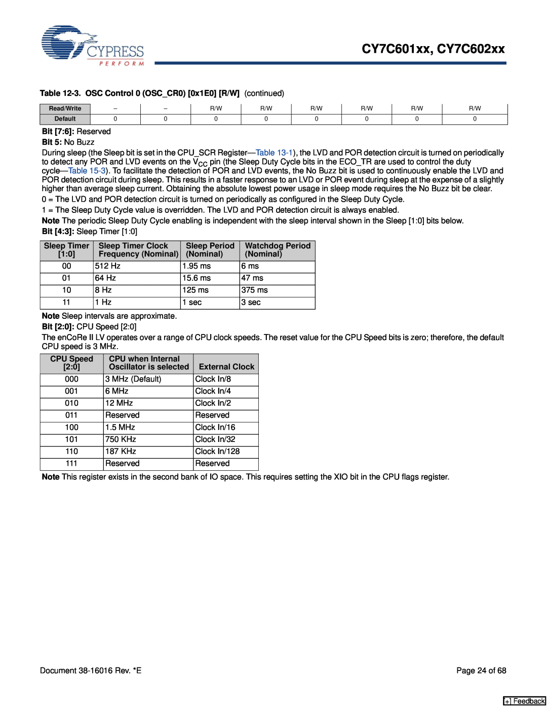
Table 12-3. OSC Control 0 OSCCR0 0x1E0 R/W
Sleep Timer
Sleep Timer Clock
CPU when Internal
Table 12-3. OSC Control 0 OSCCR0 0x1E0 R/W continued
Table 12-4. Clock IO Configuration CLKIOCR 0x32 R/W
12.2.2 Interval Timer Clock ITMRCLK
Bit 75 Reserved
Figure 12-2. Programmable Interval Timer Block Diagram
12.2.3 Timer Capture Clock TCAPCLK
Figure 12-3. Timer Capture Block Diagram
Table 12-5. Timer Clock Configuration TMRCLKCR 0x31 R/W
Page 27 of
XGM Setting
12.2.4 Internal Clock Trim
Table 12-6. IOSC Trim IOSCTR 0x34 R/W
Bit 40 Gain
12.3 CPU Clock During Sleep Mode
12.2.6 LPOSC Trim
Table 12-8. LPOSC Trim LPOSCTR 0x36 R/W
13. Reset
Table 13-1. System Status and Control Register CPUSCR 0xFF R/W
Bit 7 GIES
Bit 5 WDRS
13.1 Power On Reset
13.2 Watchdog Timer Reset
Table 13-2. Reset Watchdog Timer RESWDT 0xE3 W
14. Sleep Mode
14.1.1 Low Power in Sleep Mode
14.1 Sleep Sequence
CPUCLK IOW SLEEP BRQ BRA PD
Figure 14-1. Sleep Timing
14.2 Wakeup Sequence
Figure 14-2. Wakeup Timing
15. Low Voltage Detect Control
Table 15-1. Low Voltage Control Register LVDCR 0x1E3 R/W
Bit 76 Reserved Bit 54 PORLEV10
Bit 20 VM20
15.1 POR Compare State
15.2 ECO Trim Register
Table 15-2. Voltage Monitor Comparators Register VLTCMP 0x1E4 R
Bit 72 Reserved Bit 1 LVD
16. General Purpose IO Ports
16.1 Port Data Registers
16.1.1 P0 Data
Table 16-1. P0 Data Register P0DATA0x00 R/W
16.2 GPIO Port Configuration
16.2.1 Int Enable
16.1.3 P2 Data
Table 16-3. P2 Data Register P2DATA 0x02 R/W
16.2.7 Output Enable
16.2.6 Pull Up Enable
Figure 16-1. GPIO Block Diagram
16.2.9 P0.0/CLKIN Configuration
16.2.10 P0.1/CLKOUT Configuration
Table 16-7. P0.1/CLKOUT Configuration P01CR 0x06 R/W
16.2.11 P0.2/INT0-P0.4/INT2 Configuration
16.2.12 P0.5/TIO0-P0.6/TIO1 Configuration
16.2.13 P0.7 Configuration
Table 16-10. P0.7 Configuration P07CR 0x0C R/W
16.2.14 P1.0 Configuration
16.2.15 P1.1 Configuration
Table 16-12. P1.1 Configuration P11CR 0x0E R/W
16.2.16 P1.2 Configuration
Table 16-13. P1.2 Configuration P12CR 0x0F R/W
16.2.18 P1.4-P1.6 Configuration SCLK, SMOSI, SMISO
Table 16-15. P1.4-P1.6 Configuration P14CR-P16CR 0x11-0x13 R/W
16.2.19 P1.7 Configuration
Table 16-16. P1.7 Configuration P17CR 0x14 R/W
16.2.21 P3 Configuration
Table 16-18. P3 Configuration P3CR 0x16 R/W
16.2.22 P4 Configuration
Table 16-19. P4 Configuration P4CR 0x17 R/W
Figure 17-1. SPI Block Diagram
17. Serial Peripheral Interface SPI
17.2 SPI Configure Register
Table 17-2. SPI Configure Register SPICR 0x3D R/W
17.1 SPI Data Register
Table 17-1. SPI Data Register SPIDATA 0x3C R/W
Table 17-3. SPI Mode Timing vs. LSB First, CPOL, and CPHA
Diagram
CPHA
CPOL
18. Timer Registers
17.3 SPI Interface Pins
Figure 18-1. 16-Bit Free Running Counter Block Diagram
Table 18-1. Free Running Timer Low Order Byte FRTMRL 0x20 R/W
Table 18-2. Free Running Timer High Order Byte FRTMRH 0x21 R/W
Figure 18-2. Time Capture Block Diagram
Table 18-3. Timer Configuration TMRCR 0x2A R/W
18.1.2 Time Capture
Table 18-4. Capture Interrupt Enable TCAPINTE 0x2B R/W
Table 18-5. Timer Capture 0 Rising TCAP0R 0x22 R/W
Table 18-6. Timer Capture 1 Rising TCAP1R 0x23 R/W
Table 18-7. Timer Capture 0 Falling TCAP0F 0x24 R/W
Table 18-8. Timer Capture 1 Falling TCAP1F 0x25 R/W
18.1.3 Programmable Interval Timer
Table 18-10. Programmable Interval Timer Low PITMRL 0x26 R
Table 18-9. Capture Interrupt Status TCAPINTS 0x2C R/W
Table 18-11. Programmable Interval Timer High PITMRH 0x27 R
Table 18-12. Programmable Interval Reload Low PIRL 0x28 R/W
Table 18-13. Programmable Interval Reload High PIRH 0x29 R/W
Figure 18-3. Timer Functional Sequence Diagram
Page 52 of
Figure 18-4. 16-Bit Free Running Counter Loading Timing Diagram
Figure 18-5. Memory Mapped Registers Read and Write Timing Diagram
Figure 19-1. Interrupt Controller Block Diagram
19. Interrupt Controller
19.1 Architectural Description
Table 19-1. Interrupt Priorities, Address, and Name
19.2 Interrupt Processing
19.3 Interrupt Latency
19.4 Interrupt Registers
Table 19-2. Interrupt Clear 0 INTCLR0 0xDA R/W
Table 19-3. Interrupt Clear 1 INTCLR1 0xDB R/W
Interrupt Clear 2 INTCLR2 0xDC R/W
19.4.2 Interrupt Mask Registers
Table 19-5. Interrupt Mask 3 INTMSK3 0xDE R/W
Table 19-6. Interrupt Mask 2 INTMSK2 0xDF R/W
Table 19-7. Interrupt Mask 1 INTMSK1 0xE1 R/W
Page 57 of
Table 19-8. Interrupt Mask 0 INTMSK0 0xE0 R/W
19.4.3 Interrupt Vector Clear Register
Table 19-9. Interrupt Vector Clear Register INTVC 0xE2 R/W
20.1 DC Characteristics
20. Absolute Maximum Ratings
Parameter
Conditions
20.2 AC Characteristics
Clock
SPI Timing
Figure 20-1. Clock Timing
Figure 20-2. GPIO Timing Diagram
SCK CPOL=0
SCK CPOL=1
MOSI MISO
MOSI
MISO
SS SCK CPOL=0 SCK CPOL=1
MOSI MISO MSB
21. Ordering Information
22. Package Handling
SCK CPOL=0 SCK CPOL=1
MOSI MSB
23. Package Diagrams
Figure 23-1. 24-Pin 300-Mil SOIC S13
Figure 23-2. 24-Pin 300-Mil PDIP P13
3. DIMENSIONS IN INCHES
Figure 23-3. 24-Pin QSOP O241
Figure 23-4. 28-Pin 5.3 mm Shrunk Small Outline Package O28
Page 65 of
Figure 23-5. 40-Pin 600-Mil Molded DIP P17
Figure 23-6. 48-Pin Shrunk Small Outline Package O48
Page 66 of
24. Document History Page
Document Number
Orig. of
Submission
Sales, Solutions, and Legal Information
PSoC Solutions
Worldwide Sales and Design Support
Products
![Table 12-3. OSC Control 0 (OSC_CR0) [0x1E0] [R/W] (continued)](/images/new-backgrounds/126830/12683047x1.webp)