CY7C601xx, CY7C602xx
19.2 Interrupt Processing
The sequence of events that occur during interrupt processing is as follows:
1.An interrupt becomes active, either because:
a.The interrupt condition occurs (for example, a timer expires).
b.A previously posted interrupt is enabled through an update of an interrupt mask register.
c.An interrupt is pending and GIE is set from 0 to 1 in the CPU Flag register.
2.The current executing instruction finishes.
3.The internal interrupt is dispatched, taking 13 cycles. During this time, the following actions occur:
a.The MSB and LSB of Program Counter and Flag registers (CPU_PC and CPU_F) are stored onto the program stack by an automatic CALL instruction (13 cycles) generated during the interrupt acknowledge process.
b.The PCH, PCL, and Flag register (CPU_F) are stored onto the program stack (in that order) by an automatic CALL instruction (13 cycles) generated during the interrupt acknowledge process.
c.The CPU_F register is then cleared. Since this clears the GIE bit to 0, additional interrupts are temporarily disabled.
d.The PCH (PC[15:8]) is cleared to zero.
e.The interrupt vector is read from the interrupt controller and its value placed into PCL (PC[7:0]). This sets the program counter to point to the appropriate address in the interrupt table (for example, 0004h for the POR and LVD interrupt).
4.Program execution vectors to the interrupt table. Typically, a LJMP instruction in the interrupt table sends execution to the user's Interrupt Service Routine (ISR) for this interrupt.
5.The ISR executes. Note that interrupts are disabled since
GIE = 0. In the ISR, interrupts are
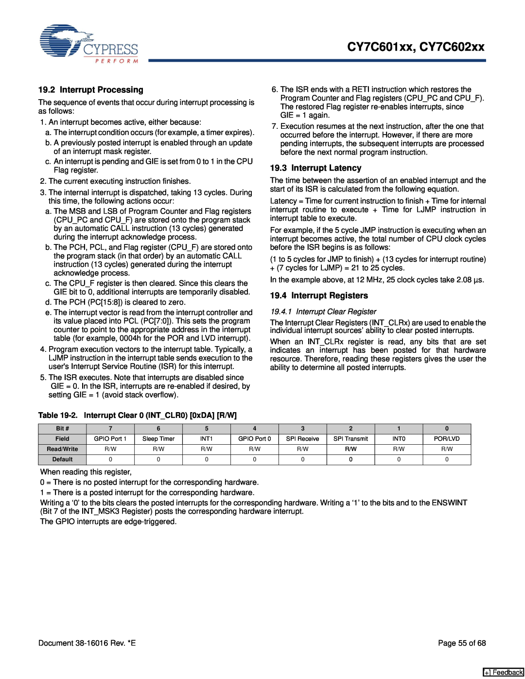
Table 19-2. Interrupt Clear 0 (INT_CLR0) [0xDA] [R/W]
6.The ISR ends with a RETI instruction which restores the Program Counter and Flag registers (CPU_PC and CPU_F). The restored Flag register
7.Execution resumes at the next instruction, after the one that occurred before the interrupt. However, if there are more pending interrupts, the subsequent interrupts are processed before the next normal program instruction.
19.3 Interrupt Latency
The time between the assertion of an enabled interrupt and the start of its ISR is calculated from the following equation.
Latency = Time for current instruction to finish + Time for internal interrupt routine to execute + Time for LJMP instruction in interrupt table to execute.
For example, if the 5 cycle JMP instruction is executing when an interrupt becomes active, the total number of CPU clock cycles before the ISR begins is as follows:
(1 to 5 cycles for JMP to finish) + (13 cycles for interrupt routine) + (7 cycles for LJMP) = 21 to 25 cycles.
In the example above, at 12 MHz, 25 clock cycles take 2.08 µs.
19.4 Interrupt Registers
19.4.1 Interrupt Clear Register
The Interrupt Clear Registers (INT_CLRx) are used to enable the individual interrupt sources’ ability to clear posted interrupts.
When an INT_CLRx register is read, any bits that are set indicates an interrupt has been posted for that hardware resource. Therefore, reading these registers gives the user the ability to determine all posted interrupts.
Bit # | 7 | 6 | 5 | 4 | 3 | 2 | 1 | 0 |
Field | GPIO Port 1 | Sleep Timer | INT1 | GPIO Port 0 | SPI Receive | SPI Transmit | INT0 | POR/LVD |
Read/Write | R/W | R/W | R/W | R/W | R/W | R/W | R/W | R/W |
Default | 0 | 0 | 0 | 0 | 0 | 0 | 0 | 0 |
|
|
|
|
|
|
|
|
|
When reading this register,
0 = There is no posted interrupt for the corresponding hardware.
1 = There is a posted interrupt for the corresponding hardware.
Writing a ‘0’ to the bits clears the posted interrupts for the corresponding hardware. Writing a ‘1’ to the bits and to the ENSWINT (Bit 7 of the INT_MSK3 Register) posts the corresponding hardware interrupt.
The GPIO interrupts are
Document | Page 55 of 68 |
[+] Feedback