CY7C6431x
CY7C64345, CY7C6435x
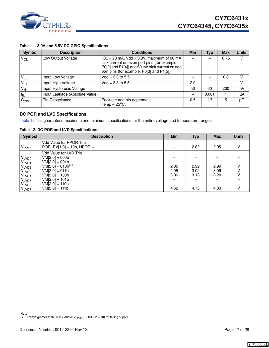
Table 11. 3.0V and 5.5V DC GPIO Specifications
Symbol | Description | Conditions | Min | Typ | Max | Units |
VOL | Low Output Voltage | IOL = 20 mA, Vdd > 3.3V, maximum of 60 mA | – | – | 0.75 | V |
|
| sink current on even port pins (for example, |
|
|
|
|
|
| P0[2] and P1[4]) and 60 mA sink current on odd |
|
|
|
|
|
| port pins (for example, P0[3] and P1[5]). |
|
|
|
|
VIL | Input Low Voltage | Vdd = 3.3 to 5.5. | – | – | 0.8 | V |
VIH | Input High Voltage | Vdd = 3.3 to 5.5. | 2.0 | – |
| V |
VH | Input Hysteresis Voltage |
| 50 | 60 | 200 | mV |
IIL | Input Leakage (Absolute Value) |
| – | 0.001 | 1 | µA |
CPIN | Pin Capacitance | Package and pin dependent. | 0.5 | 1.7 | 5 | pF |
|
| Temp = 25oC. |
|
|
|
|
DC POR and LVD Specifications
Table 12 lists guaranteed maximum and minimum specifications for the entire voltage and temperature ranges.
Table 12. DC POR and LVD Specifications
Symbol | Description | Min | Typ | Max | Units |
| Vdd Value for PPOR Trip |
|
|
|
|
VPPOR | PORLEV[1:0] = 10b, HPOR = 1 | – | 2.82 | 2.95 | V |
| Vdd Value for LVD Trip | – | – | – | – |
VLVD0 | VM[2:0] = 000b | ||||
VLVD1 | VM[2:0] = 001b | – | – | – | – |
VLVD2 | VM[2:0] = 010b(7) | 2.85 | 2.92 | 2.99 | V |
VLVD3 | VM[2:0] = 011b | 2.95 | 3.02 | 3.09 | V |
VLVD4 | VM[2:0] = 100b | 3.06 | 3.13 | 3.20 | V |
VLVD5 | VM[2:0] = 101b | – | – | – | – |
VLVD6 | VM[2:0] = 110b | – | – | – | – |
VLVD7 | VM[2:0] = 111b | 4.62 | 4.73 | 4.83 | V |
Note
7. Always greater than 50 mV above VPPOR (PORLEV = 10) for falling supply.
Document Number: | Page 17 of 28 |
[+] Feedback
