CY7C6431x
CY7C64345, CY7C6435x
AC General Purpose I/O Specifications
Table 17 lists guaranteed maximum and minimum specifications for the entire voltage and temperature ranges.
Table 17. AC GPIO Specifications
Symbol | Description | Conditions |
| Min | Typ | Max | Units |
FGPIO | GPIO Operating Frequency | Normal Strong Mode, Ports 0, 1 | 0 | – | 12 | MHz | |
TRise23 | Rise Time, Strong Mode | Vdd = 3.3 to 5.5V, 10% | - 90% | 15 | – | 80 | ns |
| Ports 2, 3 |
|
|
|
|
|
|
TRise01 | Rise Time, Strong Mode | Vdd = 3.3 to 5.5V, 10% | - 90% | 10 | – | 50 | ns |
| Ports 0, 1 |
|
|
|
|
|
|
TFall | Fall Time, Strong Mode | Vdd = 3.3 to 5.5V, 10% | - 90% | 10 | – | 50 | ns |
| All Ports |
|
|
|
|
|
|
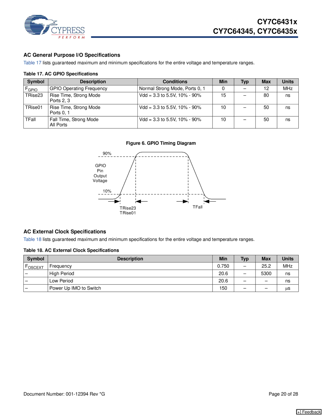
Figure 6. GPIO Timing Diagram
90% |
|
GPIO |
|
Pin |
|
Output |
|
Voltage |
|
10% |
|
TRise23 | TFall |
TRise01 |
|
AC External Clock Specifications
Table 18 lists guaranteed maximum and minimum specifications for the entire voltage and temperature ranges.
Table 18. AC External Clock Specifications
Symbol | Description | Min | Typ | Max | Units |
FOSCEXT | Frequency | 0.750 | – | 25.2 | MHz |
– | High Period | 20.6 | – | 5300 | ns |
– | Low Period | 20.6 | – | – | ns |
– | Power Up IMO to Switch | 150 | – | – | μs |
Document Number: | Page 20 of 28 |
[+] Feedback