CY7C6431x
CY7C64345, CY7C6435x
DC Programming Specifications
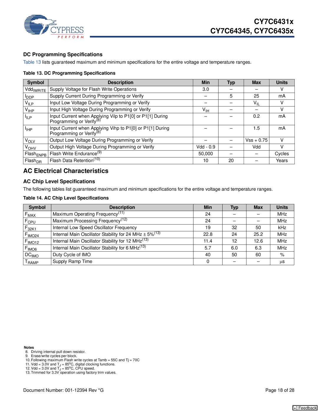
Table 13 lists guaranteed maximum and minimum specifications for the entire voltage and temperature ranges.
Table 13. DC Programming Specifications
Symbol | Description | Min | Typ | Max | Units |
VddIWRITE | Supply Voltage for Flash Write Operations | 3.0 | – | – | V |
IDDP | Supply Current During Programming or Verify | – | 5 | 25 | mA |
VILP | Input Low Voltage During Programming or Verify | – | – | VIL | V |
VIHP | Input High Voltage During Programming or Verify | VIH | – | – | V |
IILP | Input Current when Applying Vilp to P1[0] or P1[1] During | – | – | 0.2 | mA |
| Programming or Verify(8) |
|
|
|
|
IIHP | Input Current when Applying Vihp to P1[0] or P1[1] During | – | – | 1.5 | mA |
| Programming or Verify(8) |
|
|
|
|
VOLV | Output Low Voltage During Programming or Verify | – | – | Vss + 0.75 | V |
VOHV | Output High Voltage During Programming or Verify | Vdd - 0.9 | – | Vdd | V |
FlashENPB | Flash Write Endurance(9) | 50,000 | – | – | Cycles |
FlashDR | Flash Data Retention(10) | 10 | 20 | – | Years |
AC Electrical Characteristics
AC Chip Level Specifications
The following tables list guaranteed maximum and minimum specifications for the entire voltage and temperature ranges.
Table 14. AC Chip Level Specifications
Symbol | Description | Min | Typ | Max | Units |
FMAX | Maximum Operating Frequency(11) | 24 | – | – | MHz |
FCPU | Maximum Processing Frequency(12) | 24 | – | – | MHz |
F32K1 | Internal Low Speed Oscillator Frequency | 19 | 32 | 50 | kHz |
FIMO24 | Internal Main Oscillator Stability for 24 MHz ± 5%(13) | 22.8 | 24 | 25.2 | MHz |
FIMO12 | Internal Main Oscillator Stability for 12 MHz(13) | 11.4 | 12 | 12.6 | MHz |
FIMO6 | Internal Main Oscillator Stability for 6 MHz(13) | 5.7 | 6.0 | 6.3 | MHz |
DCIMO | Duty Cycle of IMO | 40 | 50 | 60 | % |
TRAMP | Supply Ramp Time | 0 | – | – | μs |
Notes
8.Driving internal pull down resistor.
9.Erase/write cycles per block.
10.Following maximum Flash write cycles at Tamb = 55C and Tj = 70C
11.Vdd = 3.0V and TJ = 85oC, digital clocking functions.
12.Vdd = 3.0V and TJ = 85oC, CPU speed.
13.Trimmed for 3.3V operation using factory trim values.
Document Number: | Page 18 of 28 |
[+] Feedback
