CY8C21634, CY8C21534

CY8C21434, CY8C21334, CY8C21234

Absolute Maximum Ratings

Table 12. Absolute Maximum Ratings

Symbol

Description

Min

Typ

Max

Units

Notes

TSTG

Storage Temperature

-55

25

+100

oC

Higher storage temperatures


reduce data retention time. Recom-


mended storage temperature is


+25oC ± 25oC. Extended duration


storage temperatures above 65oC


degrade reliability.

TA

Ambient Temperature with Power Applied

-40

+85

oC


Vdd

Supply Voltage on Vdd Relative to Vss

-0.5

+6.0

V


VIO

DC Input Voltage

Vss -

Vdd +

V


0.5


0.5


VIOZ

DC Voltage Applied to Tri-state

Vss -

Vdd +

V


0.5


0.5


IMIO

Maximum Current into any Port Pin

-25

+50

mA


ESD

Electro Static Discharge Voltage

2000

V

Human Body Model ESD.

LU

Latch-up Current

200

mA


Operating Temperature


Table 13.

Operating Temperature


Symbol

Description

Min

Typ

Max

Units

Notes

TA

Ambient Temperature

-40

+85

oC


TJ

Junction Temperature

-40

+100

oC

The temperature rise from ambient


to junction is package specific. See


Table 40 on page 38. The user must


limit the power consumption to


comply with this requirement.

DC Electrical Characteristics

DC Chip-Level Specifications

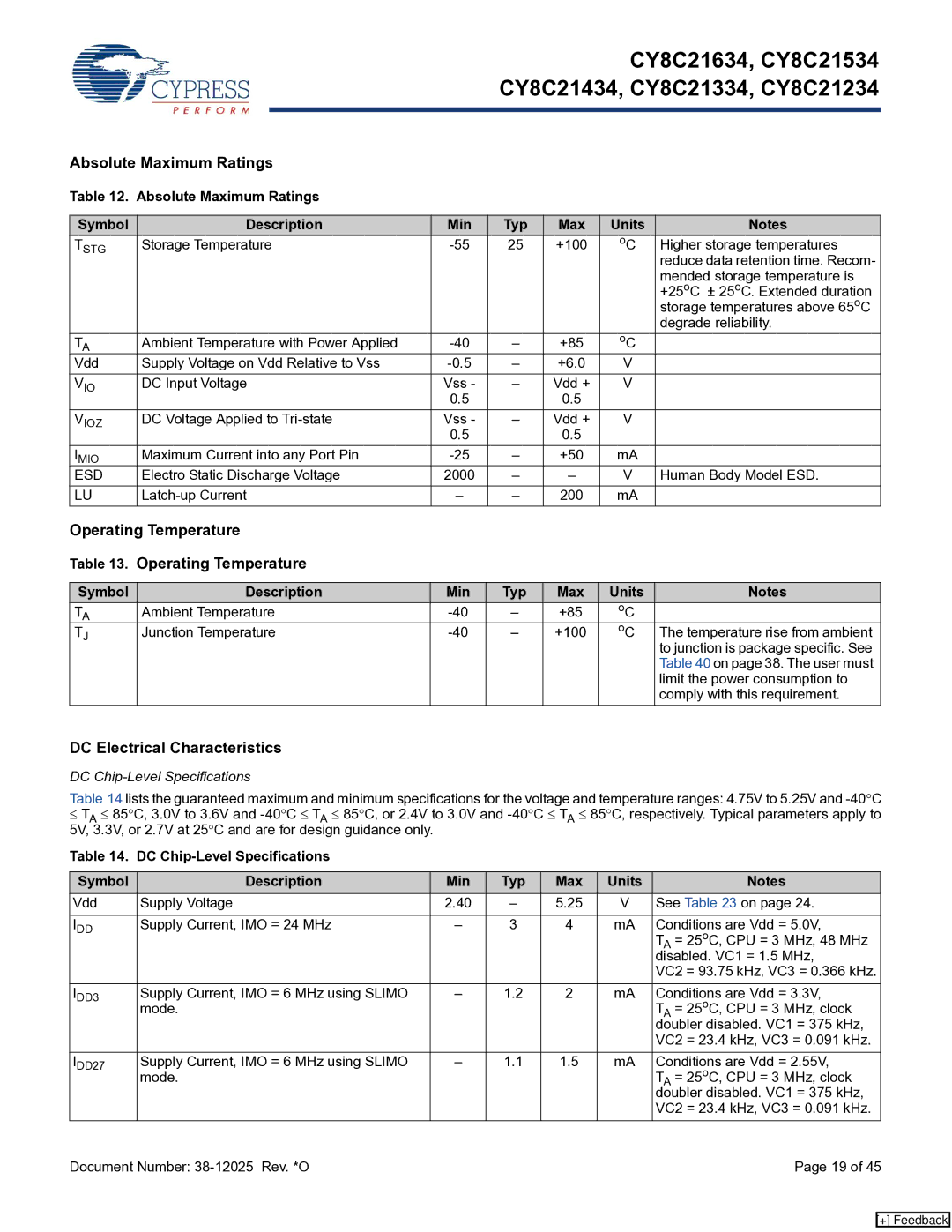
Table 14 lists the guaranteed maximum and minimum specifications for the voltage and temperature ranges: 4.75V to 5.25V and -40°C

TA 85°C, 3.0V to 3.6V and -40°C TA 85°C, or 2.4V to 3.0V and -40°C TA 85°C, respectively. Typical parameters apply to 5V, 3.3V, or 2.7V at 25°C and are for design guidance only.

Table 14. DC Chip-Level Specifications

Symbol

Description

Min

Typ

Max

Units

Notes

Vdd

Supply Voltage

2.40

5.25

V

See Table 23 on page 24.


IDD

Supply Current, IMO = 24 MHz

3

4

mA

Conditions are Vdd = 5.0V,


TA = 25oC, CPU = 3 MHz, 48 MHz


disabled. VC1 = 1.5 MHz,


VC2 = 93.75 kHz, VC3 = 0.366 kHz.

IDD3

Supply Current, IMO = 6 MHz using SLIMO

1.2

2

mA

Conditions are Vdd = 3.3V,


mode.


TA = 25oC, CPU = 3 MHz, clock


doubler disabled. VC1 = 375 kHz,


VC2 = 23.4 kHz, VC3 = 0.091 kHz.

IDD27

Supply Current, IMO = 6 MHz using SLIMO

1.1

1.5

mA

Conditions are Vdd = 2.55V,


mode.


TA = 25oC, CPU = 3 MHz, clock


doubler disabled. VC1 = 375 kHz,


VC2 = 23.4 kHz, VC3 = 0.091 kHz.

Document Number: 38-12025 Rev. *O


Page 19 of 45

[+] Feedback

Page 19
Image 19
Cypress CY8C21534, CY8C21334, CY8C21634 manual Absolute Maximum Ratings, Operating Temperature, DC Electrical Characteristics

CY8C21634, CY8C21534, CY8C21434, CY8C21334, CY8C21234 specifications

The Cypress CY8C21234, CY8C21334, CY8C21434, CY8C21534, and CY8C21634 are members of the PSoC® 1 family of microcontrollers, designed for embedded applications that demand flexibility, integration, and efficiency. These microcontrollers are well-suited for a variety of projects due to their unique characteristics and advanced technologies.

One of the primary features of the PSoC 1 series is the integration of analog and digital components on a single chip. This combination allows for the implementation of complex control algorithms without the need for multiple external components. Each device in this family is equipped with programmable analog blocks capable of interfacing with sensors, as well as digital blocks that facilitate communication with various peripherals.

The CY8C21234 series provides a 16-bit architecture, which enhances performance for processing and control tasks. The microcontrollers boast an operational range of up to 24 MHz, making them suitable for high-speed applications. With up to 16 KB of flash memory, these devices have ample memory for storing program code and user data.

Another key characteristic of the CY8C21234, CY8C21334, CY8C21434, CY8C21534, and CY8C21634 devices is their ease of use. They come with a comprehensive development environment known as PSoC Designer. This software provides a user-friendly interface to configure the device’s hardware resources graphically and allows for seamless integration of custom firmware.

In terms of communication capabilities, these microcontrollers support multiple protocols, including I²C, SPI, and UART, providing versatile interfacing options with other devices. This makes them ideal for applications such as sensor processing, motor control, and portable devices.

Power management is another significant highlight of the PSoC 1 family. The microcontrollers are designed with low-power operation in mind, featuring multiple sleep modes that contribute to extended battery life in portable applications.

Overall, the Cypress CY8C21234, CY8C21334, CY8C21434, CY8C21534, and CY8C21634 microcontrollers are a versatile solution for a wide range of embedded applications, combining programmable analog and digital components, ease of development, and efficient power management in a compact form factor. Their performance and flexibility make them a popular choice among engineers and developers exploring innovative designs.