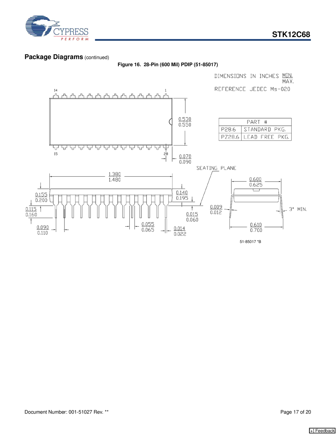
Contents
STK12C68
Features
Functional Description
Cypress Semiconductor Corporation
Pin Definitions
Pin Configurations
Write Enable Input, Active LOW. When the chip is enabled and
Output Enable, Active LOW. The active LOW
SRAM Read
Device Operation
SRAM Write
AutoStore Operation
Hardware RECALL Power Up
AutoStore Inhibit Mode
Figure 3. AutoStore Inhibit Mode
Hardware STORE HSB Operation
Data Protection
Low Average Active Power
Noise Considerations
Hardware Protect
Table 1. Hardware Mode Selection
Best Practices
Power
STK12C68
Maximum Ratings
DC Electrical Characteristics
Operating Range
STK12C68
Data Retention and Endurance
STK12C68
Capacitance
Thermal Resistance
Switching Waveforms
AC Switching Characteristics
SRAM Read Cycle
STK12C68
STK12C68
SRAM Write Cycle
Switching Waveforms
Switching Waveform
AutoStore or Power Up RECALL
Low Voltage Trigger VSWITCH to
STK12C68
Switching Waveform
Software Controlled STORE/RECALL Cycle
STK12C68
17. The software sequence is clocked on the falling edge of CE without involving OE double clocking aborts the sequence
Switching Waveform
Hardware STORE Cycle
STK12C68
+ Feedback
Ordering Information
Part Numbering nomenclature STK12C68 - S F 45 I TR
Package Diagram
STK12C68
STK12C68
Ordering Information continued
Package Diagram
STK12C68
Package Diagrams
Figure 14. 28-Pin 330 Mil SOIC
Figure 15. 28-Pin 300 Mil PDIP
STK12C68
Package Diagrams continued
Figure 16. 28-Pin 600 Mil PDIP
+ Feedback
STK12C68
Package Diagrams continued
Figure 17. 28-Pin 300 Mil Side Braze DIL
Page 18 of
1. ALL DIMENSION ARE IN INCHES AND MILLIMETERS MIN/MAX
Package Diagrams continued
2. JEDEC 95 OUTLINE# MO-041 3. PACKAGE WEIGHT TBD
STK12C68
PSoC Solutions
Sales, Solutions, and Legal Information
Document History Page
Worldwide Sales and Design Support