VCAP ![]() A16
A16 ![]() A14
A14 ![]()
A12 ![]()
A7 ![]()
A6 ![]()
A5 ![]()
INT ![]()
A4 ![]()
NC
NC
NC
VSS
NC
VRTCbat
DQ 0 ![]()
A3 ![]()
A2 ![]()
A1 ![]()
A0 ![]()
DQ 1 ![]()
DQ 2 ![]()
X1 ![]()
X2 ![]()
![]()
148 ![]() V CC
V CC
247 ![]() A15
A15
346 ![]() HSB
HSB
445 ![]()
![]() W
W
544 ![]() A13
A13
643 ![]() A8
A8
742 ![]() A9
A9
841 ![]() NC
NC
940 ![]() A11
A11
10 | (TOP) | 39 |
| NC |
11 | 38 |
| NC | |
| ||||
| ||||
12 |
| 37 |
| NC |
|
| |||
|
| |||
13 |
| 36 |
| V SS |
|
| |||
|
|
1435 ![]() NC
NC
1534 ![]() V RTCcap
V RTCcap
1633 ![]() DQ 6
DQ 6
1732 ![]() G
G
1831 ![]() A10
A10
1930 ![]() E
E
2029 ![]() DQ 7
DQ 7
2128 ![]() DQ 5
DQ 5
2227 ![]() DQ 4
DQ 4
2326 ![]() DQ 3
DQ 3
2425 ![]() V CC
V CC
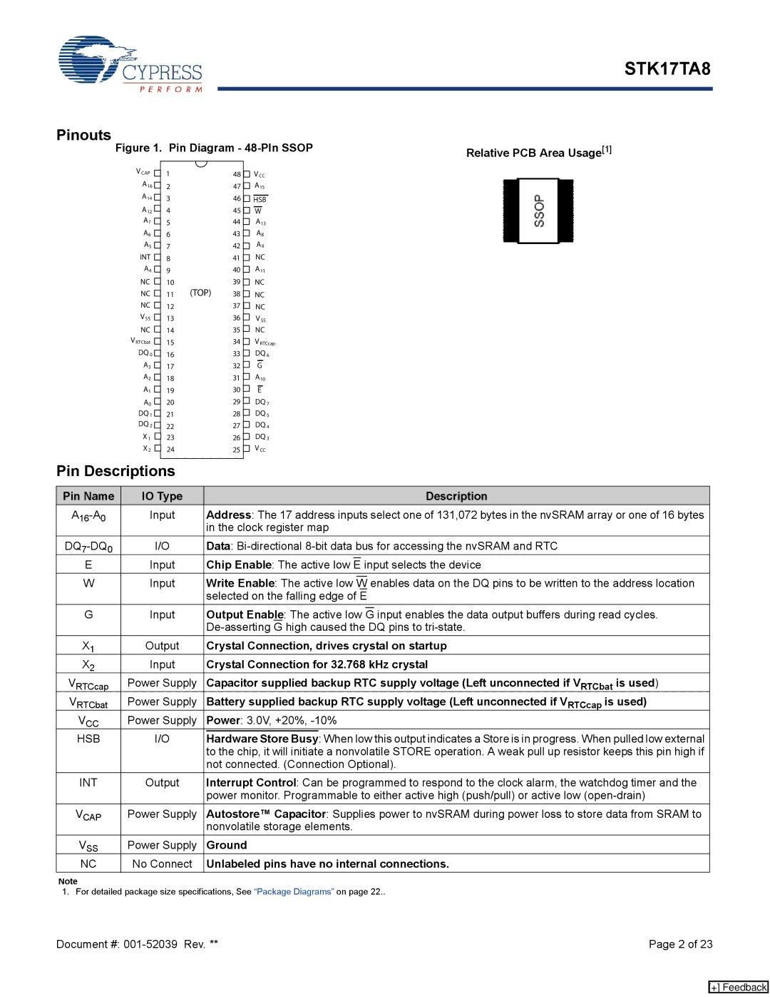
Pin Descriptions
Pin Name | IO Type |
|
| Description |
| Input | Address: The 17 address inputs select one of 131,072 bytes in the nvSRAM array or one of 16 bytes | ||
|
| in the clock register map | ||
I/O | Data: | |||
E | Input | Chip Enable: The active low |
| input selects the device |
E | ||||
WInput Write Enable: The active low W enables data on the DQ pins to be written to the address location selected on the falling edge of E
GInput Output Enable: The active low G input enables the data output buffers during read cycles.
X1 | Output | Crystal Connection, drives crystal on startup | |
X2 | Input | Crystal Connection for 32.768 kHz crystal | |
VRTCcap | Power Supply | Capacitor supplied backup RTC supply voltage (Left unconnected if VRTCbat is used) | |
VRTCbat | Power Supply | Battery supplied backup RTC supply voltage (Left unconnected if VRTCcap is used) | |
VCC | Power Supply | Power: 3.0V, +20%, | |
HSB | I/O |
| : When low this output indicates a Store is in progress. When pulled low external |
Hardware Store Busy | |||
|
| to the chip, it will initiate a nonvolatile STORE operation. A weak pull up resistor keeps this pin high if | |
|
| not connected. (Connection Optional). | |
INT | Output | Interrupt Control: Can be programmed to respond to the clock alarm, the watchdog timer and the | |
|
| power monitor. Programmable to either active high (push/pull) or active low | |
VCAP | Power Supply | Autostore™ Capacitor: Supplies power to nvSRAM during power loss to store data from SRAM to | |
|
| nonvolatile storage elements. | |
VSS | Power Supply | Ground | |
NC | No Connect | Unlabeled pins have no internal connections. | |
Note
1. For detailed package size specifications, See “Package Diagrams” on page 22..
Document #: | Page 2 of 23 |
[+] Feedback