Z8 Encore!® Flash Microcontroller Development Kit
User Manual
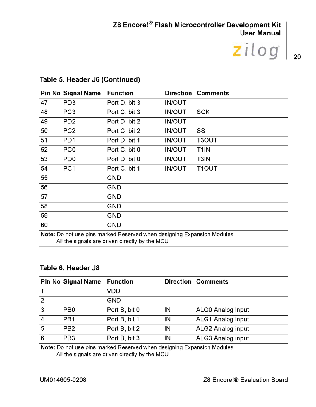
Table 5. Header J6 (Continued)
20
Pin No Signal Name | Function | Direction | Comments | |
47 | PD3 | Port D, bit 3 | IN/OUT |
|
|
|
|
|
|
48 | PC3 | Port C, bit 3 | IN/OUT | SCK |
|
|
|
|
|
49 | PD2 | Port D, bit 2 | IN/OUT |
|
|
|
|
|
|
50 | PC2 | Port C, bit 2 | IN/OUT | SS |
|
|
|
|
|
51 | PD1 | Port D, bit 1 | IN/OUT | T3OUT |
|
|
|
|
|
52 | PC0 | Port C, bit 0 | IN/OUT | T1IN |
|
|
|
|
|
53 | PD0 | Port D, bit 0 | IN/OUT | T3IN |
|
|
|
|
|
54 | PC1 | Port C, bit 1 | IN/OUT | T1OUT |
|
|
|
|
|
55 |
| GND |
|
|
|
|
|
|
|
56 |
| GND |
|
|
|
|
|
|
|
57 |
| GND |
|
|
|
|
|
|
|
58 |
| GND |
|
|
|
|
|
|
|
59 |
| GND |
|
|
|
|
|
|
|
60 |
| GND |
|
|
| ||||
Note: Do not use pins marked Reserved when designing Expansion Modules. | ||||
| All the signals are driven directly by the MCU. |
| ||
Table 6. Header J8
Pin No Signal Name | Function | Direction | Comments | |
1 |
| VDD |
|
|
|
|
|
|
|
2 |
| GND |
|
|
|
|
|
|
|
3 | PB0 | Port B, bit 0 | IN | ALG0 Analog input |
|
|
|
|
|
4 | PB1 | Port B, bit 1 | IN | ALG1 Analog input |
|
|
|
|
|
5 | PB2 | Port B, bit 2 | IN | ALG2 Analog input |
|
|
|
|
|
6 | PB3 | Port B, bit 3 | IN | ALG3 Analog input |
Note: Do not use pins marked Reserved when designing Expansion Modules. All the signals are driven directly by the MCU.
Z8 Encore!® Evaluation Board |