2 SYSTEM OVERVIEW
2.1 Hardware Overview
The Mark III CMU is based upon the Multiple Application Processing System (MAPS) platform which is the new generation hardware that will be used for introduction of new Honeywell datalink products. This common hardware platform will facilitate the introduction of communication products that integrate new capabilities with the Mark III CMU.
The Mark III CMU is a single Line Replaceable Unit (LRU) housed in a standard 4 MCU ARINC 600 form factor. The Mark III CMU contains 4 Circuit Card Assemblies (CCAs): (1) Processor; (2) I/O; (3) Power Supply; and (4) Interconnect. There is expansion capacity for two spare CCAs.
The main processor is a 266 MHz Pentium while the I/O is handled by two MPC 860 microprocessors. These two I/O processors are able to concurrently process all I/O effectively eliminating throughput bottlenecks. Additionally, there are two dedicated digital signal processors (DSPs), one each for the VHF and UHF modems. There is a total of 64 MB of DRAM along with 48 MB of Flash EPROM.
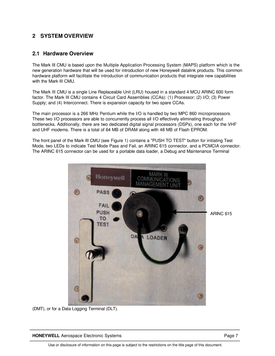
The front panel of the Mark III CMU (see Figure 1) contains a "PUSH TO TEST" button for initiating Test Mode, two LEDs to indicate Test Mode Pass and Fail, an ARINC 615 connector, and a PCMCIA connector. The ARINC 615 connector can be used for a portable data loader, a Debug and Maintenance Terminal
ARINC 615
(DMT), or for a Data Logging Terminal (DLT).
HONEYWELL Aerospace Electronic Systems | Page 7 |
Use or disclosure of information on this page is subject to the restrictions on the title page of this document.