HEADQUARTERS, Department of the Army
TM 11-6625-2779-14&P
Reporting Errors and Recommending Improvements
Technical Manual Headquarters Department of the Army
NSN
Replaceable Parts
List of Illustrations
List of Tables
Iii
Maintenance Forms, Records, and Reports
Section Introduction
Scope
Administrative Storage
Destruction of Army Electronics Materiel
Reporting Equipment Improvement Recommendations EIR
Items Comprising an Operable Equipment
Voice Frequency Level Measurements 20Hz to 20kHz
Specifications
Section General Information Introduction
Section
Accessory Equipment Supplied
Accessory Equipment Supplied
Instrument Identification
BAL Modification
Warranty Exception
Section Installation Inspection
Power Requirements
Battery
Cover Removal
Installation and Removal of Battery
Battery
Controls Connectors Indicators
Section
Operating Instructions
Front Panel Controls, Indicators, and Connectors
Front, Side and Rear Pane
Side Panel Controls and Connectors
Level Measurements
Level and Noise Measurements
Page
Noise Measurement
Applications
Recorder Compatibility
Recorder Compatibility Chart
Transmission Loss Measurements
Identifying Noise Characteristics
Crosstalk Measurements
Crosstalk Correction Factor
Measurements in DBC
0dBm
Reinstall the set in its case
Input jacks are connected in parallel. If a 600 ohm
135 BAL
Level Measurement Noise Metallic Measurements
Step Procedure
Recorder Calibration
Noise-to-Ground Measurements Balance Measurement
Example
Transmission Loss Measurement
Section Theory of Operation Introduction
Block Diagram Description
Simplified Dial BAT Function
Detailed Circuit Description
Range Attenuator A2
Input Amplifier A3. Schematic No
FILTERS. Schematic No
Setting Attenuation
Range Attenuator
Pads Used
KHz Flat and Program Weighting Curves
C-MSG and 1SkHz Flat Weighting Curves
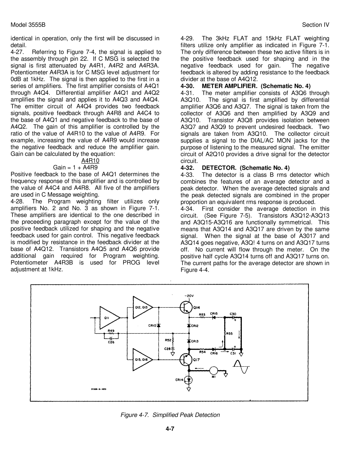
DETECTOR. Schematic No
Meter AMPLIFIER. Schematic No
Power Supply and Series Regulator Schematic No
Instrument Recommended Type Required Characteristics Model
Section Maintenance Introouction
Factory Selected Values
BAL Conversion
Level Accuracy Checks
Performance Checks
Function CARRIER, 75 Unbal
TMS, Term
Range
Unbal Carrier Accuracy Check
Frequency
30Hz to 1MHz 100Hz to 600kHz 1MHz to 3MHz
20Hz to 20kHz 40Hz to 15kHz 100Hz to 20kHz 100Hz to 15kHz
Return Loss Check
Return Loss Test Set-Up
Filter Response Checks
Filter Response Checks
MSG dBm 3kHz Flat dBm 15kHz Flat dBm Program dBm
Bridging Loss
Input Balance
TMS Brdg
Input TMS Brdg
Power Supply Check
Adjustment and Calibration Procedure
Unbal Calibration
Attenuator Calibration
Frequency Response Adjustment
Common Mode Adjustment
Balance Check
Assembly Removal
Troubleshooting Procedures
Filter Calibration
Troubleshooting Tree
Dial BAT
Front Panel Trouble Analysis
Function Troubleshooting
Front Panel Troubleshooting
Range Troubleshooting
Front Panel Trouble Analysis Contd
Filter Troubleshooting
Troubleshooting Input Amplifier
Troubleshooting the Meter Amplifier and Detector
Defective Function
Function Input Jacks DIAL/AC MON Jacks
Function Switch Resistance Values
Tip to Ring Tip to Ground Ring to Ground
Brdg Term
11. Factory Selected Values
10. Resistance Checks
Range dBm Pin 1 to Pin 2 to
Description Check
Performance Check Test Card
Carrier 75 Unbal Level Accuracy Check
Carrier 135 BAL Level Accuracy Check
Carrier 600 BAL Level Accuracy Check
Performance Check Test Card Contd
Filter Response Checks MSG
Return Loss Check
Program
Bridging Loss Check
Ordering Information
Section Replaceable Parts Introduction
03555-66507 PC Board Assy function
Replaceable Parts
03555-66508 Board Assy amplifier
Replaceable Parts Contd
A3 Contd
03555-66506 PC Board Assy filter
A4 Contd
Chassis Mounted Components
Miscellaneous
Chassis Mounted Components Contd
Miscellaneous Contd
Part Number National Stock Number Cross Reference Index
Replacement National Part Stock Number Fscm
Fscm
National Stock Number
Page
Model 3555B Appendix a
Code List of Manufacturers
Functional Block Diagram
Circuit Diagrams
Schematic Diagrams
Reference Designations
Section Model 3555B
7-4
Functional Block Diagram
7-6
A1 Function Assembly Schematic and Component Location
7-8
7-10
A4 Filter Schematic and Component Location
11/7-12
References
Appendix a
Maintenance Function
Maintenance Allocation Section I. Introduction General
Appendix B
Column Entries
Remarks Sec
Tool and Test Equipment Requiremen ts Sec
Audio Level Meter TA-885/U
REF Code Number
TM 11-7725-2779-14&P
Appendix C
Manual Backdating Changes
Transmission and Noise Measuring SET
Government Printing Office 1980-603-128/66
Delete CR6 across M1
Chief of Staff
General, United States Army
Major General, United States Army Adjutant General
Active Army
Page
PIN