SMA Connectors
The output clock SMA connector provides a signal that can be used to phase lock a signal source. The frequency is that of the input clock signal divided by 2. For example, with an attached CLC5958 ADC evaluation board at 52MSPS the clock output signal will be a 26MHz square wave. The second SMA connector is currently unused.
Serial Port
The serial port is configured at 115,200 baud with one stop bit, no parity, and
Power Up the System
Once the WCLK jumper and the DIP switches have been set, (for example, for the CLC5956 we have set WCLK at RDY2 and DIP switches 1,2,3,4,5 as ON,ON,ON,OFF,OFF) connect the evaluation board to the data capture board, apply power, clock, and signal to the boards, and connect the serial cable to the PC. Some PCs will need to be rebooted at this point, but it may not be necessary with your PC. In the software configuration section, next, we will check the communication between the PC and the data capture board.
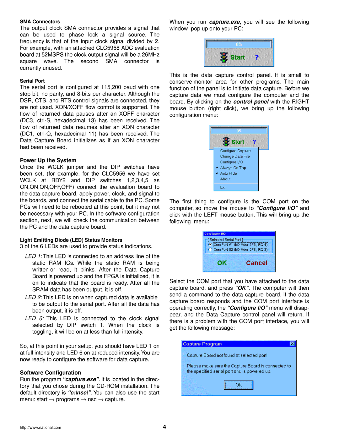
When you run capture.exe, you will see the following window pop up onto your PC:
This is the data capture control panel. It is small to conserve monitor area for other programs. The main function of the panel is to initiate data capture. Before we capture data we must configure the computer and the board. By clicking on the control panel with the RIGHT mouse button (right click), we bring up the following configuration menu:
The first thing to configure is the COM port on the computer, so move the mouse to “Configure I/O” and click with the LEFT mouse button. This will bring up the following menu:
Light Emitting Diode (LED) Status Monitors
3 of the 6 LEDs are used to provide status indications.
LED 1: This LED is connected to an address line of the static RAM ICs. While the static RAM is being written or read, it blinks. After the Data Capture Board is powered up and the FPGA is initialized, it is on to indicate that the board is ready. After all the SRAM data has been output, it is off.
LED 2: This LED is on when captured data is available to be output to the serial port. After all the data has been output, it is off.
LED 6: This LED is connected to the clock signal selected by DIP switch 1. When the clock is toggling, it will be on at less than full intensity.
So, at this point in your setup, you should have LED 1 on at full intensity and LED 6 on at reduced intensity. You are now ready to configure the software for data capture.
Software Configuration
Run the program “capture.exe”. It is located in the direc- tory that you chose during the
http://www.national.com | 4 |
Select the COM port that you have attached to the data capture board, and press “OK”. The computer will then send a command to the data capture board. If the data capture board responds and the COM port interface is operating correctly, the “Configure I/O” menu will disap- pear, and the Data Capture control panel will return. If there is a problem with the COM port interface, you will get the following message: