#4 & #5 as indicated in the Histogram Max Target table. Due to a high data resolution and relatively slow data rate, a relatively long period of time is required for generating histogram data from the DRCS with high decimation values in the DDC. Under some circumstances, the serial PC interface will time out. The program detects this condition and queries the user to continue. Click “Yes” to continue and wait for the Progress Bar to run to completion. Be patient, it could take several minutes depending on the input amplitude and DDC decimation value and Histogram Target Value. The last mode description, Debug Histogram, provides further description of the output file generated by the hard- wired histogram generator.
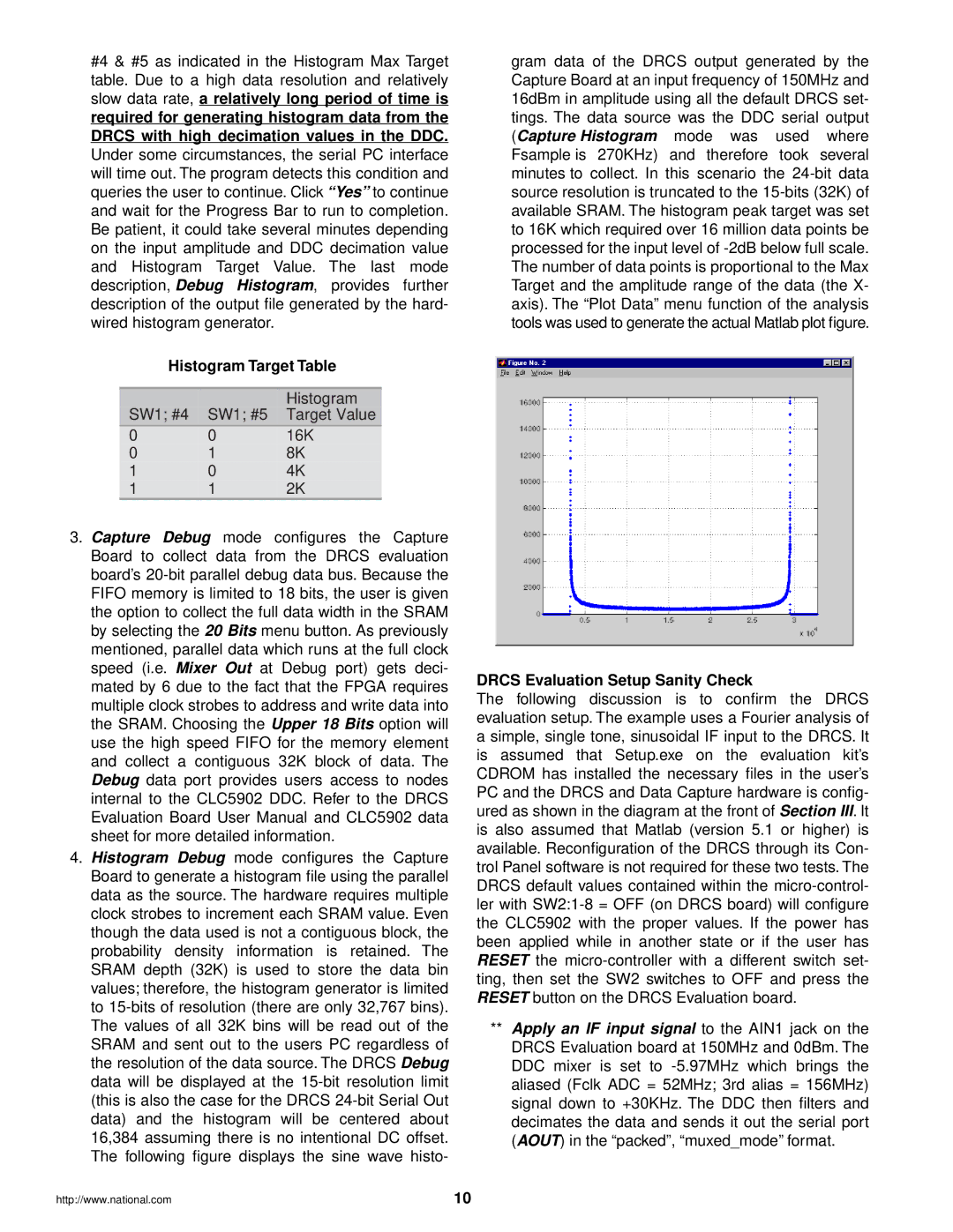
gram data of the DRCS output generated by the Capture Board at an input frequency of 150MHz and 16dBm in amplitude using all the default DRCS set- tings. The data source was the DDC serial output (Capture Histogram mode was used where Fsample is 270KHz) and therefore took several minutes to collect. In this scenario the
Histogram Target Table
|
| Histogram |
SW1; #4 | SW1; #5 | Target Value |
0 | 0 | 16K |
0 | 1 | 8K |
1 | 0 | 4K |
1 | 1 | 2K |
3.Capture Debug mode configures the Capture Board to collect data from the DRCS evaluation board’s
4.Histogram Debug mode configures the Capture Board to generate a histogram file using the parallel data as the source. The hardware requires multiple clock strobes to increment each SRAM value. Even though the data used is not a contiguous block, the probability density information is retained. The SRAM depth (32K) is used to store the data bin values; therefore, the histogram generator is limited to
DRCS Evaluation Setup Sanity Check
The following discussion is to confirm the DRCS evaluation setup. The example uses a Fourier analysis of a simple, single tone, sinusoidal IF input to the DRCS. It is assumed that Setup.exe on the evaluation kit’s CDROM has installed the necessary files in the user’s PC and the DRCS and Data Capture hardware is config- ured as shown in the diagram at the front of Section III. It is also assumed that Matlab (version 5.1 or higher) is available. Reconfiguration of the DRCS through its Con- trol Panel software is not required for these two tests. The DRCS default values contained within the
**Apply an IF input signal to the AIN1 jack on the DRCS Evaluation board at 150MHz and 0dBm. The DDC mixer is set to
http://www.national.com | 10 |