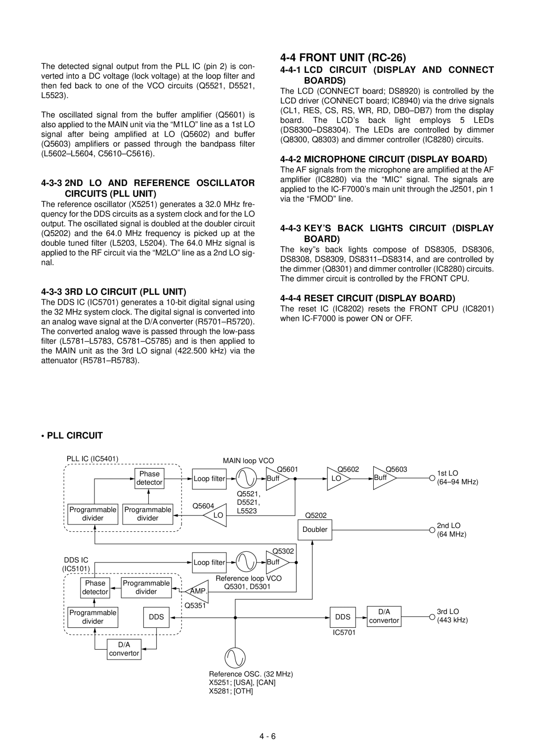
The detected signal output from the PLL IC (pin 2) is con- verted into a DC voltage (lock voltage) at the loop filter and then fed back to one of the VCO circuits (Q5521, D5521, L5523).
The oscillated signal from the buffer amplifier (Q5601) is also applied to the MAIN unit via the “M1LO” line as a 1st LO signal after being amplified at LO (Q5602) and buffer (Q5603) amplifiers or passed through the bandpass filter
4-3-3 2ND LO AND REFERENCE OSCILLATOR CIRCUITS (PLL UNIT)
The reference oscillator (X5251) generates a 32.0 MHz fre- quency for the DDS circuits as a system clock and for the LO output. The oscillated signal is doubled at the doubler circuit (Q5202) and the 64.0 MHz frequency is picked up at the double tuned filter (L5203, L5204). The 64.0 MHz signal is applied to the RF circuit via the “M2LO” line as a 2nd LO sig- nal.
4-4 FRONT UNIT (RC-26)
4-4-1 LCD CIRCUIT (DISPLAY AND CONNECT BOARDS)
The LCD (CONNECT board; DS8920) is controlled by the LCD driver (CONNECT board; IC8940) via the drive signals (CL1, RES, CS, RS, WR, RD,
4-4-2 MICROPHONE CIRCUIT (DISPLAY BOARD)
The AF signals from the microphone are amplified at the AF amplifier (IC8280) via the “MIC” signal. The signals are applied to the
4-4-3 KEY’S BACK LIGHTS CIRCUIT (DISPLAY BOARD)
The key”s back lights compose of DS8305, DS8306, DS8308, DS8309,
4-3-3 3RD LO CIRCUIT (PLL UNIT)
The DDS IC (IC5701) generates a
4-4-4 RESET CIRCUIT (DISPLAY BOARD)
The reset IC (IC8202) resets the FRONT CPU (IC8201) when
• PLL CIRCUIT
PLL IC (IC5401) |
|
|
|
|
|
|
|
|
| MAIN loop VCO |
|
|
|
|
| |||||||||||
|
|
|
|
|
|
|
|
|
|
|
|
|
|
|
|
|
| Q5601 |
|
| Q5602 | Q5603 | ||||
|
|
|
|
|
| Phase |
|
|
|
|
|
|
| |||||||||||||
|
|
|
|
|
|
|
|
|
| Loop filter |
|
|
| Buff |
|
|
|
| LO |
| Buff | |||||
|
|
|
|
|
| detector |
|
|
|
|
|
|
|
|
|
|
| |||||||||
|
|
|
|
|
|
|
|
|
|
|
|
|
|
|
|
|
|
|
|
|
|
|
|
| ||
|
|
|
|
|
|
|
|
|
|
|
|
|
|
|
| Q5521, |
|
|
|
|
|
|
| |||
|
|
|
|
|
|
|
|
|
|
|
|
|
|
|
|
|
|
|
|
|
| |||||
|
|
|
|
|
|
|
|
|
|
|
|
|
|
|
|
|
|
|
| |||||||
|
|
|
|
|
|
|
|
|
|
|
| Q5604 |
| D5521, |
|
|
|
|
|
| ||||||
| Programmable |
| Programmable |
|
|
|
| L5523 |
|
|
|
|
|
|
| |||||||||||
|
|
|
|
|
| LO |
|
|
| Q5202 |
| |||||||||||||||
| divider |
|
|
| divider |
|
|
|
|
|
|
|
|
|
|
|
|
| ||||||||
|
|
|
|
|
|
|
|
|
|
|
|
|
|
|
|
| Doubler |
|
|
| ||||||
|
|
|
|
|
|
|
|
|
|
|
|
|
|
|
|
|
|
|
|
|
|
|
|
| ||
|
|
|
|
|
|
|
|
|
|
|
|
|
|
|
|
|
|
|
|
|
|
|
|
| ||
|
|
|
|
|
|
|
|
|
|
|
|
|
|
|
|
|
|
|
|
|
|
|
|
|
|
|
1st LO
(64 94 MHz)
2nd LO (64 MHz)
|
|
|
| Q5302 | |
DDS IC |
| Loop filter | Buff | ||
(IC5101) |
|
|
|
| |
Phase | Programmable |
| Reference loop VCO | ||
AMP. | Q5301, D5301 | ||||
detector | divider | ||||
|
| ||||
Programmable |
| Q5351 |
|
| |
DDS |
|
|
| ||
divider |
|
|
| ||
|
|
|
| ||
D/A
convertor
D/A
DDS ![]() convertor
convertor
IC5701
3rd LO (443 kHz)
Reference OSC. (32 MHz) X5251; [USA], [CAN] X5281; [OTH]
4 - 6