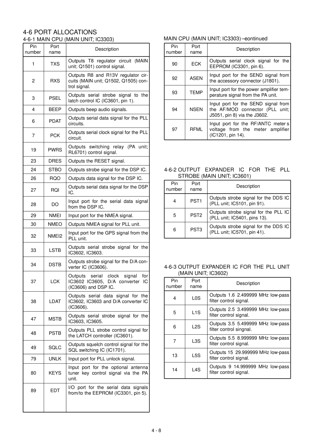
4-6 PORT ALLOCATIONS
4-6-1 MAIN CPU (MAIN UNIT; IC3303)
Pin | Port | Description | |
number | name | ||
| |||
|
|
| |
1 | TXS | Outputs T8 regulator circuit (MAIN | |
unit; Q1501) control signal. | |||
|
| ||
|
|
| |
|
| Outputs R8 and R13V regulator cir- | |
2 | RXS | cuits (MAIN unit; Q1502, Q1505) con- | |
|
| trol signal. | |
|
|
| |
3 | PSEL | Outputs serial strobe signal to the | |
latch control IC (IC3601, pin 1). | |||
|
| ||
|
|
| |
4 | BEEP | Outputs beep audio signals. | |
|
|
| |
6 | PDAT | Outputs serial data signal for the PLL | |
circuits. | |||
|
| ||
|
|
| |
7 | PCK | Outputs serial clock signal for the PLL | |
circuit. | |||
|
| ||
|
|
| |
19 | PWRS | Outputs switching relay (PA unit; | |
RL6701) control signal. | |||
|
| ||
|
|
| |
23 | DRES | Outputs the RESET signal. | |
|
|
| |
24 | STBO | Outputs strobe signal for the DSP IC. | |
|
|
| |
26 | RQO | Outputs data signal for the DSP IC. | |
|
|
| |
27 | RQI | Outputs serial data signal for the DSP | |
IC. | |||
|
| ||
|
|
| |
28 | DO | Input port for the serial data signal | |
from the DSP IC. | |||
|
| ||
|
|
| |
29 | NMEI | Input port for the NMEA signal. | |
|
|
| |
30 | NMEO | Outputs NMEA signal for PLL unit. | |
|
|
| |
32 | NMEI2 | Input port for the GPS signal from the | |
PLL unit. | |||
|
| ||
|
|
| |
33 | LSTB | Outputs serial strobe signal for the | |
IC3602, IC3603. | |||
|
| ||
|
|
| |
34 | DSTB | Outputs strobe signal for the D/A con- | |
verter IC (IC3606). | |||
|
| ||
|
|
| |
|
| Outputs serial clock signal for | |
37 | LCK | ||
|
| (IC3606) and DSP IC. | |
|
|
| |
|
| Outputs serial data signal for the | |
38 | LDAT | IC3602, IC3603 and D/A converter IC | |
|
| (IC3606). | |
|
|
| |
47 | MSTB | Outputs serial strobe signal for the | |
IC3603, IC3605. | |||
|
| ||
|
|
| |
48 | PSTB | Outputs PLL strobe control signal for | |
the LATCH controller (IC3601). | |||
|
| ||
|
|
| |
49 | SQLC | Outputs squelch control signal for the | |
SQL switching IC (IC1701). | |||
|
| ||
|
|
| |
79 | UNLK | Input port for PLL unlock signal. | |
|
|
| |
|
| Input port for the optional antenna | |
80 | KEYS | tuner key control signal via the PA | |
|
| unit. | |
|
|
| |
89 | EDT | I/O port for the serial data signals | |
from/to the EEPROM (IC3301, pin 5). | |||
|
| ||
|
|
|
MAIN CPU (MAIN UNIT;
Pin | Port | Description | |
number | name | ||
| |||
|
|
| |
90 | ECK | Outputs serial clock signal for the | |
EEPROM (IC3301, pin 6). | |||
|
| ||
|
|
| |
92 | ASEN | Input port for the SEND signal from | |
the accessory connector (J1801). | |||
|
| ||
|
|
| |
93 | TEMP | Input port for the power amplifier tem- | |
perature signal from the PA unit. | |||
|
| ||
|
|
| |
|
| Input port for the SEND signal from | |
94 | NSEN | the AF/MOD connector (PLL unit; | |
|
| J5051, pin 8) via the J3602. | |
|
|
| |
|
| Input port for the RF/ANTC meter’s | |
97 | RFML | voltage from the meter amplifier | |
|
| (IC1201, pin 14). | |
|
|
|
4-6-2 OUTPUT EXPANDER IC FOR THE PLL STROBE (MAIN UNIT; IC3601)
Pin | Port | Description | |
number | name | ||
| |||
|
|
| |
4 | PST1 | Outputs strobe signal for the DDS IC | |
(PLL unit; IC5101, pin 91). | |||
|
| ||
|
|
| |
5 | PST2 | Outputs strobe signal for the PLL IC | |
(PLL unit; IC5401, pins 13). | |||
|
| ||
|
|
| |
6 | PST3 | Outputs strobe signal for the DDS IC | |
(PLL unit; IC5701, pin 41). | |||
|
| ||
|
|
|
4-6-3 OUTPUT EXPANDER IC FOR THE PLL UNIT (MAIN UNIT; IC3602)
Pin | Port | Description | |
number | name | ||
| |||
|
|
| |
4 | L0S | Outputs | |
filter control signal. | |||
|
| ||
|
|
| |
5 | L1S | Outputs | |
filter control signal. | |||
|
| ||
|
|
| |
6 | L2S | Outputs | |
filter control singnal. | |||
|
| ||
|
|
| |
7 | L3S | Outputs | |
filter control signal. | |||
|
| ||
|
|
| |
13 | L5S | Outputs | |
filter control signal. | |||
|
| ||
|
|
| |
14 | L4S | Outputs | |
filter control signal. | |||
|
| ||
|
|
|
4 - 8