Intel® 5100 MCH Chipset

1.3Related Documents

Intel® Electronic Design Kits (EDKs) provide online, real-time collateral updates. The following links take you to the EDK server and require you to log into Intel® Business Link (IBL).

Quad-Core and Dual-Core Intel® Xeon® Processor 5000 Sequence with Intel® 5100 Memory Controller Hub Chipset for Communications, Embedded, and Storage Applications

Intel® Core™2 Duo Processors T9400 and SL9400 and Intel® 5100 Memory Controller Hub Chipset for Communications and Embedded Applications

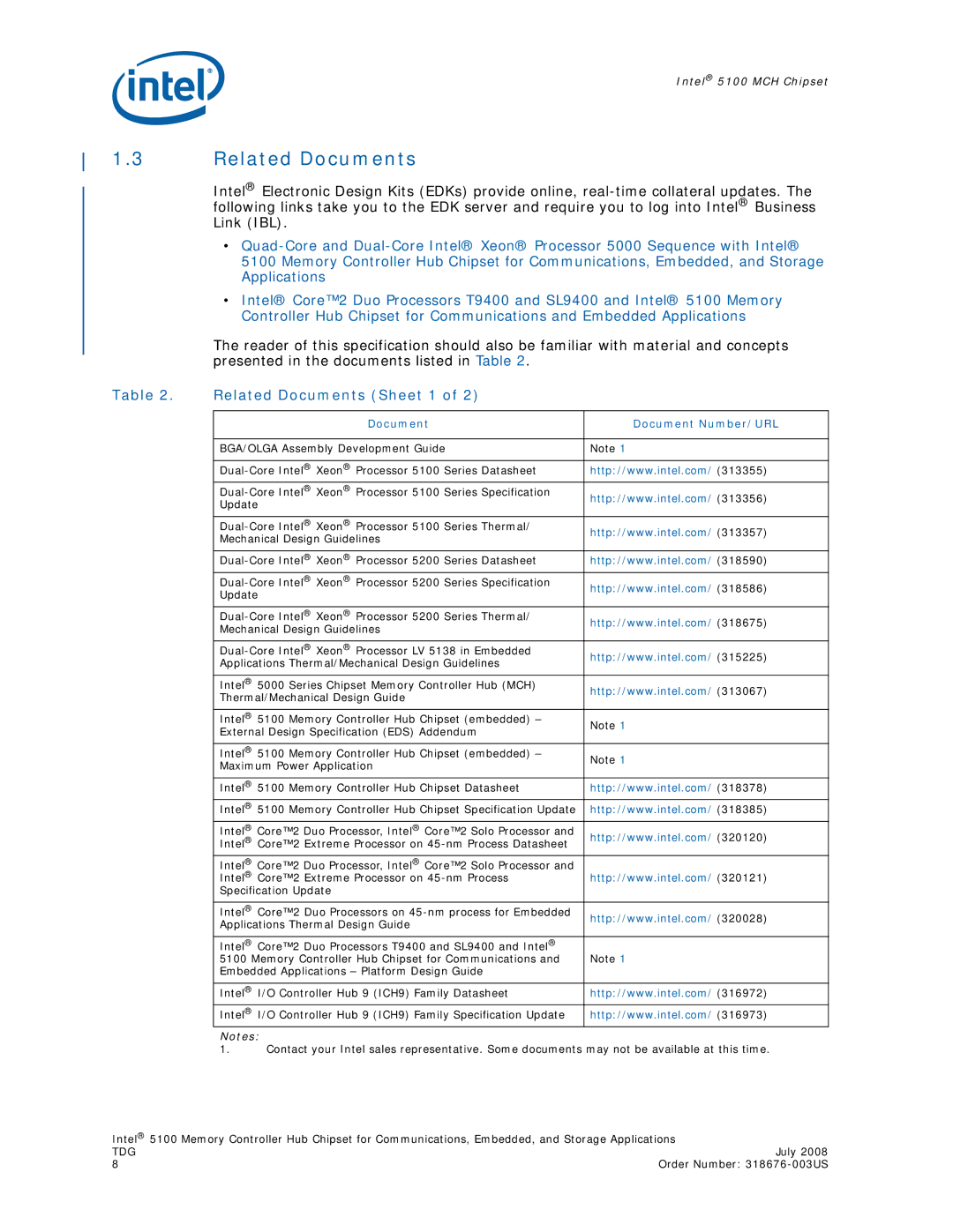
The reader of this specification should also be familiar with material and concepts presented in the documents listed in Table 2.

Table 2.

Related Documents (Sheet 1 of 2)


Document

Document Number/URL


BGA/OLGA Assembly Development Guide

Note 1


Dual-Core Intel® Xeon® Processor 5100 Series Datasheet

http://www.intel.com/ (313355)


Dual-Core Intel® Xeon® Processor 5100 Series Specification

http://www.intel.com/ (313356)


Update


Dual-Core Intel® Xeon® Processor 5100 Series Thermal/

http://www.intel.com/ (313357)


Mechanical Design Guidelines


Dual-Core Intel® Xeon® Processor 5200 Series Datasheet

http://www.intel.com/ (318590)


Dual-Core Intel® Xeon® Processor 5200 Series Specification

http://www.intel.com/ (318586)


Update


Dual-Core Intel® Xeon® Processor 5200 Series Thermal/

http://www.intel.com/ (318675)


Mechanical Design Guidelines


Dual-Core Intel® Xeon® Processor LV 5138 in Embedded

http://www.intel.com/ (315225)


Applications Thermal/Mechanical Design Guidelines


Intel® 5000 Series Chipset Memory Controller Hub (MCH)

http://www.intel.com/ (313067)


Thermal/Mechanical Design Guide


Intel® 5100 Memory Controller Hub Chipset (embedded) –

Note 1


External Design Specification (EDS) Addendum


Intel® 5100 Memory Controller Hub Chipset (embedded) –

Note 1


Maximum Power Application


Intel® 5100 Memory Controller Hub Chipset Datasheet

http://www.intel.com/ (318378)


Intel® 5100 Memory Controller Hub Chipset Specification Update

http://www.intel.com/ (318385)


Intel® Core™2 Duo Processor, Intel® Core™2 Solo Processor and

http://www.intel.com/ (320120)


Intel® Core™2 Extreme Processor on 45-nm Process Datasheet


Intel® Core™2 Duo Processor, Intel® Core™2 Solo Processor and


Intel® Core™2 Extreme Processor on 45-nm Process

http://www.intel.com/ (320121)


Specification Update


Intel® Core™2 Duo Processors on 45-nm process for Embedded

http://www.intel.com/ (320028)


Applications Thermal Design Guide


Intel® Core™2 Duo Processors T9400 and SL9400 and Intel®


5100 Memory Controller Hub Chipset for Communications and

Note 1


Embedded Applications – Platform Design Guide


Intel® I/O Controller Hub 9 (ICH9) Family Datasheet

http://www.intel.com/ (316972)


Intel® I/O Controller Hub 9 (ICH9) Family Specification Update

http://www.intel.com/ (316973)

Notes:

1.Contact your Intel sales representative. Some documents may not be available at this time.

Intel® 5100 Memory Controller Hub Chipset for Communications, Embedded, and Storage Applications

TDG

July 2008

8

Order Number: 318676-003US

Page 8
Image 8
Intel 5100 manual Related Documents Sheet 1, Document Document Number/URL

5100 specifications

The Intel 5100, officially known as the Intel Core 2 Duo Processor T5100, is a notable entry in Intel's line of mobile processors, designed primarily for laptops and portable computing devices. Released in early 2007, it targets users seeking a balance between performance and energy efficiency.

At its core, the Intel 5100 features a dual-core architecture that allows it to handle multiple tasks simultaneously, significantly improving multitasking capabilities compared to single-core processors. Clocked at a speed of 1.6 GHz, it provides robust performance for everyday computing tasks such as web browsing, document editing, and casual gaming.

One of the key technologies integrated into the Intel 5100 is Intel's 64-bit architecture, which enables the processor to utilize more than 4GB of RAM, catering to modern computing needs. This feature is particularly beneficial for users running demanding applications or multitasking, as it provides increased processing power and efficiency.

The Intel 5100 also incorporates Intel's Enhanced Intel SpeedStep Technology, which optimizes power consumption by dynamically adjusting the processor's frequency and voltage based on workload. This not only extends battery life in portable devices but also helps in reducing heat output, promoting a cooler computing experience.

Another significant aspect of the Intel 5100 is its support for Intel Virtualization Technology (VT-x). This feature allows multiple operating systems to run concurrently on the same machine, making it an excellent choice for developers and IT professionals who require virtual environments for testing and development purposes.

The processor is built on a 65nm process technology, which contributes to its energy efficiency and thermal management. With a Thermal Design Power (TDP) of just 35 watts, it remains within a reasonable thermal envelope, suitable for laptop designs without requiring excessive cooling solutions.

In terms of connectivity, the Intel 5100 supports a range of communication technologies. It is commonly paired with Intel’s 965GM chipset, which enhances graphics capabilities through Intel GMA X3100 integrated graphics, offering decent performance for standard visual tasks.

Overall, the Intel 5100 represents a solid choice for users seeking a combination of performance, efficiency, and advanced features, making it a reliable processor option for laptops in the mid to late 2000s. With its dual-core capabilities, 64-bit support, and energy-efficient design, it paved the way for future developments in mobile computing technology.