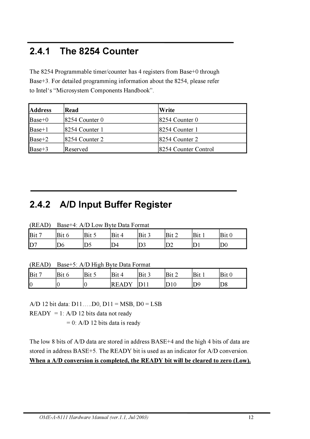
2.4.1The 8254 Counter
The 8254 Programmable timer/counter has 4 registers from Base+0 through Base+3. For detailed programming information about the 8254, please refer to Intel‘s “Microsystem Components Handbook”.
Address | Read | Write | |
Base+0 | 8254 Counter 0 | 8254 | Counter 0 |
Base+1 | 8254 Counter 1 | 8254 | Counter 1 |
Base+2 | 8254 Counter 2 | 8254 | Counter 2 |
Base+3 | Reserved | 8254 | Counter Control |
2.4.2A/D Input Buffer Register
(READ) | Base+4: A/D Low Byte Data Format |
|
|
| |||
Bit 7 | Bit 6 | Bit 5 | Bit 4 | Bit 3 | Bit 2 | Bit 1 | Bit 0 |
D7 | D6 | D5 | D4 | D3 | D2 | D1 | D0 |
(READ) | Base+5: A/D High Byte Data Format |
|
|
| |||
Bit 7 | Bit 6 | Bit 5 | Bit 4 | Bit 3 | Bit 2 | Bit 1 | Bit 0 |
0 | 0 | 0 | READY | D11 | D10 | D9 | D8 |
A/D 12 bit data: D11…..D0, D11 = MSB, D0 = LSB
READY = 1: A/D 12 bits data not ready
= 0: A/D 12 bits data is ready
The low 8 bits of A/D data are stored in address BASE+4 and the high 4 bits of data are stored in address BASE+5. The READY bit is used as an indicator for A/D conversion.
When a A/D conversion is completed, the READY bit will be cleared to zero (Low).
12 |