2.4.7A/D Multiplex Control Register
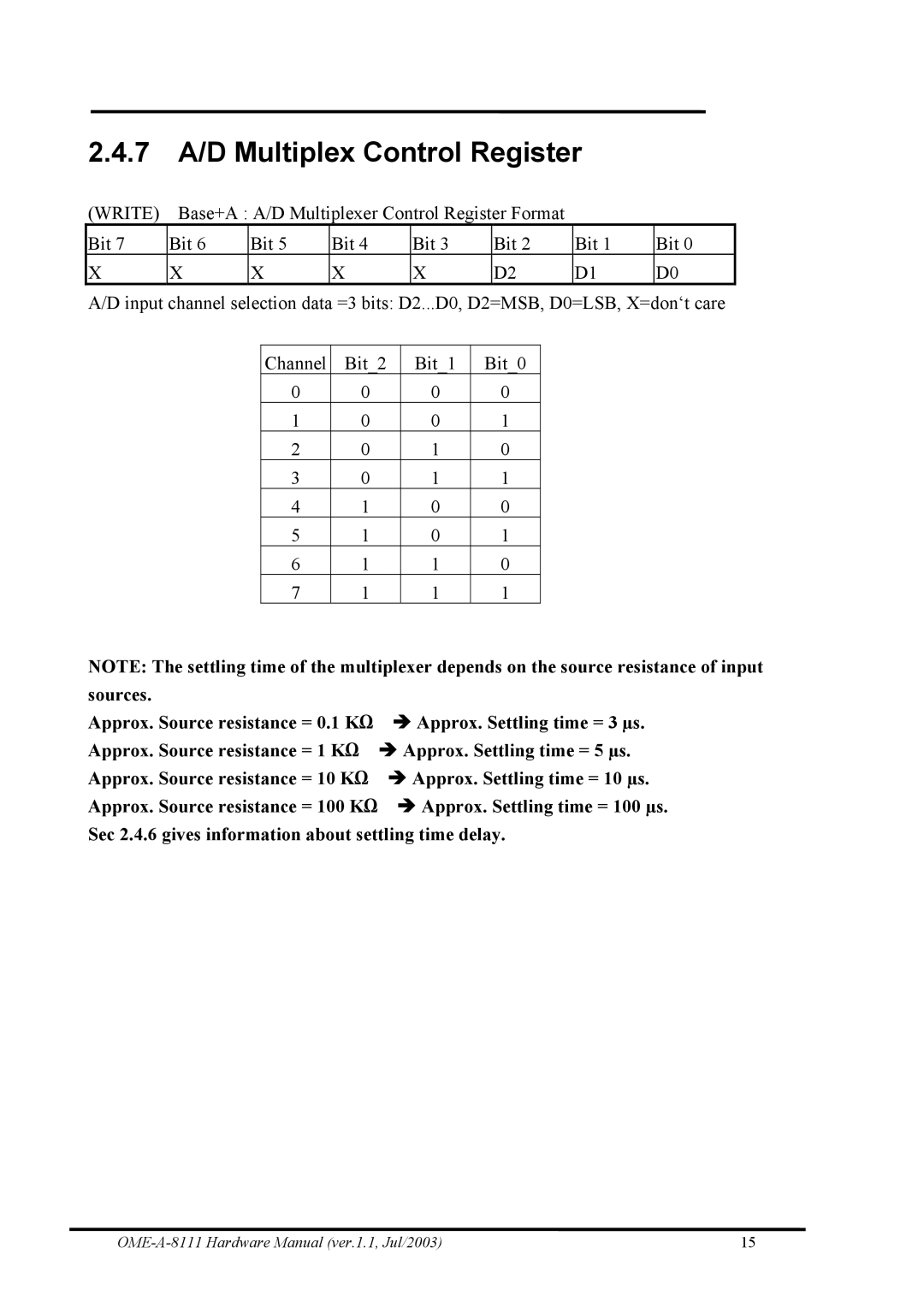
(WRITE) | Base+A : A/D Multiplexer Control Register Format |
|
| ||||
Bit 7 | Bit 6 | Bit 5 | Bit 4 | Bit 3 | Bit 2 | Bit 1 | Bit 0 |
X | X | X | X | X | D2 | D1 | D0 |
A/D input channel selection data =3 bits: D2...D0, D2=MSB, D0=LSB, X=don‘t care
Channel | Bit_2 | Bit_1 | Bit_0 |
0 | 0 | 0 | 0 |
1 | 0 | 0 | 1 |
2 | 0 | 1 | 0 |
3 | 0 | 1 | 1 |
4 | 1 | 0 | 0 |
5 | 1 | 0 | 1 |
6 | 1 | 1 | 0 |
7 | 1 | 1 | 1 |
NOTE: The settling time of the multiplexer depends on the source resistance of input
sources. |
|
|
Approx. Source resistance = 0.1 KΩ | Î Approx. Settling time = | 3 µs. |
Approx. Source resistance = 1 KΩ | Î Approx. Settling time = 5 | µs. |
Approx. Source resistance = 10 KΩ | Î Approx. Settling time = 10 µs. | |
Approx. Source resistance = 100 KΩ | Î Approx. Settling time = 100 µs. | |
Sec 2.4.6 gives information about settling time delay.
15 |