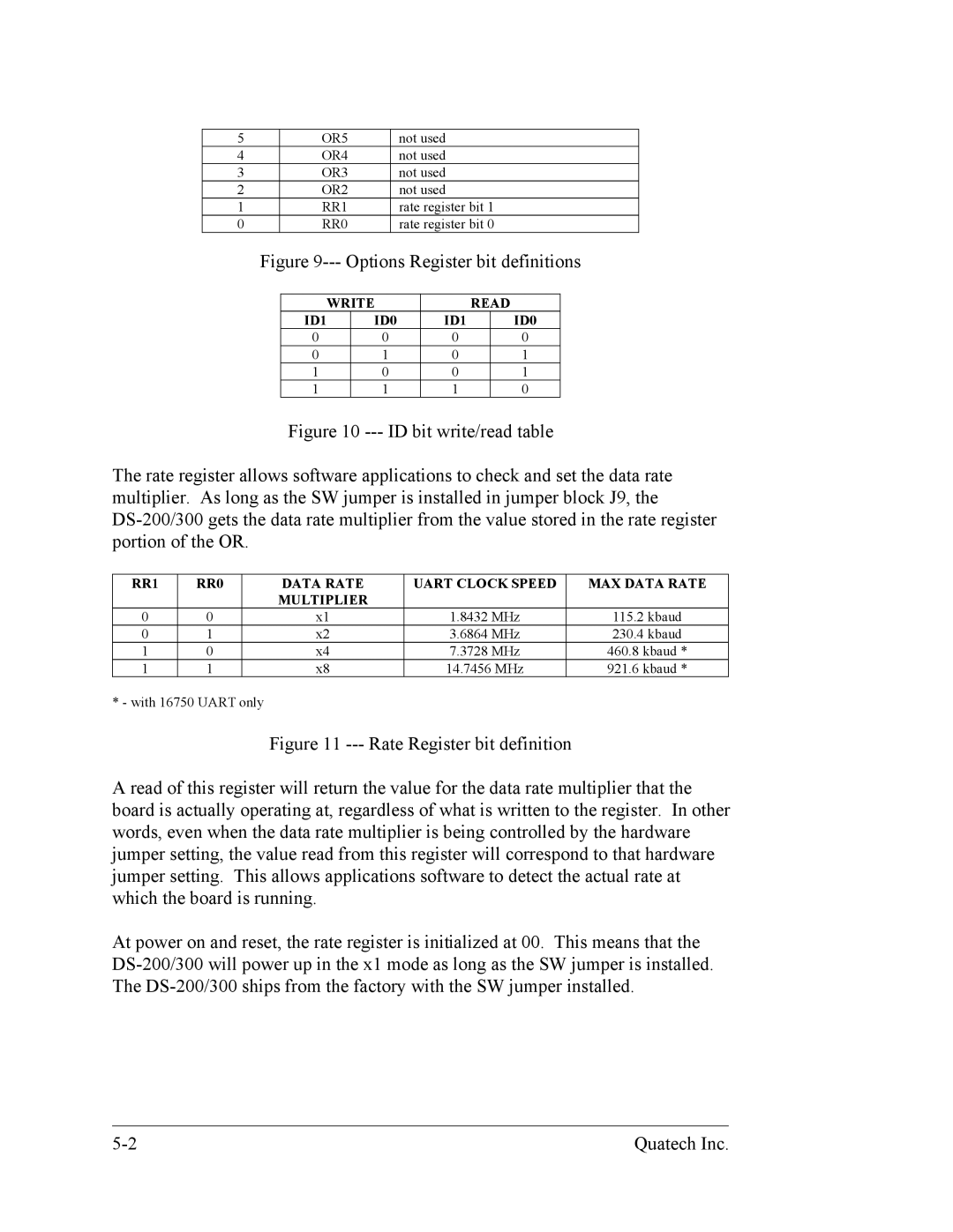
5 |
| OR5 |
|
| not used |
|
| ||
4 |
| OR4 |
|
| not used |
|
| ||
3 |
| OR3 |
|
| not used |
|
| ||
2 |
| OR2 |
|
| not used |
|
| ||
1 |
| RR1 |
|
| rate register bit 1 |
|
| ||
0 |
| RR0 |
|
| rate register bit 0 |
|
| ||
Figure | |||||||||
|
|
|
|
|
|
| |||
|
| WRITE |
| READ |
|
| |||
| ID1 | ID0 |
| ID1 |
| ID0 |
| ||
| 0 |
| 0 |
|
| 0 |
| 0 |
|
| 0 |
| 1 |
|
| 0 |
| 1 |
|
| 1 |
| 0 |
|
| 0 |
| 1 |
|
| 1 |
| 1 |
|
| 1 |
| 0 |
|
Figure 10 --- ID bit write/read table
The rate register allows software applications to check and set the data rate multiplier. As long as the SW jumper is installed in jumper block J9, the DS-200/300 gets the data rate multiplier from the value stored in the rate register portion of the OR.
RR1 | RR0 | DATA RATE | UART CLOCK SPEED | MAX DATA RATE |
|
| MULTIPLIER |
|
|
0 | 0 | x1 | 1.8432 MHz | 115.2 kbaud |
0 | 1 | x2 | 3.6864 MHz | 230.4 kbaud |
1 | 0 | x4 | 7.3728 MHz | 460.8 kbaud * |
1 | 1 | x8 | 14.7456 MHz | 921.6 kbaud * |
* - with 16750 UART only
Figure 11 --- Rate Register bit definition
A read of this register will return the value for the data rate multiplier that the board is actually operating at, regardless of what is written to the register. In other words, even when the data rate multiplier is being controlled by the hardware jumper setting, the value read from this register will correspond to that hardware jumper setting. This allows applications software to detect the actual rate at which the board is running.
At power on and reset, the rate register is initialized at 00. This means that the DS-200/300 will power up in the x1 mode as long as the SW jumper is installed. The DS-200/300 ships from the factory with the SW jumper installed.
Quatech Inc. |