Electronic Volume and Tone Control IC for Car Audio Systems
LC75411E/W 


Overview
The LC75411E/W is an electronic volume and tone control IC that implements a rich set of audio control functions with a minimal number of external components. Functions include volume, balance, fader, bass/treble, and loudness controls, as well as input selection/switching functions and an input gain control.
Electronic Volumeume andand ToneTone ControlControl ICIC forfor Car Audio Systemsems
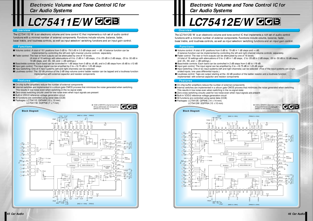
LC75412E/W2E/W 


Overview
The LC75412E/W is an electronic volume and tone control IC that implements a rich set of audio control functions with a minimal number of external components. Functions include volume, balance, fader, bass/treble, and loudness controls, as well as input selection/switching functions and an input gain control.
Functions
■Volume control: A total of 161 positions from 0 dB to
■Fader control: The rear or front outputs can be attenuated by one of 16 levels
(A total of 16 settings with attenuations of 0 to
■Bass/treble controls: Each band can be controlled in 1 dB steps from 0 dB to ±6 dB, and in 2 dB steps from ±8 dB to ±12 dB
■Input gain control: The input signal can be amplified by 0 to +18.75 dB in 1.25 dB steps
■Input switching: One of 4 input systems (left and right channels) can be selected
■Loudness control: The
Features
Functions
■Volume control: A total of 81 positions from 0 dB to
A balance function can be implemented by controlling the left and right channel volume controls separately.
■Fader control: The rear or front outputs can be attenuated by one of 16 levels
(A total of 16 settings with attenuations of 0 to
■Bass/treble controls: Each band can be controlled in 2 dB steps from 0 dB to ±18 dB
■Input gain control: The input signal can be amplified by 0 to +18.75 dB in 1.25 dB steps
■Input switching: One of six input systems (left and right channels) can be selected (Five of the input systems are single- ended inputs, one uses differential inputs.)
■Loudness control: Taps are output starting at the
Features
■
■Internal switches are implemented in a silicon gate CMOS process that minimizes the noise generated when switching. This results in low noise even when switching in the
■
■
■All functions are controlled using serial data (CCB)
■Packages: LC75411E: QIP44M (10 ![]() 10 mm)
10 mm)
LC75411W: SQFP48 (7 ![]() 7 mm)
7 mm)
❋ :CCB is SANYO's original bus format. All bus addresses are managed by SANYO for this format.
Block Diagram
■
■Internal switches are implemented in a silicon gate CMOS process that minimizes the noise generated when switching. This results in low noise even when switching in the
■
■
■All functions are controlled using serial data (CCB)
■Packages: LC75412E: QIP64E (14 ![]() 14 mm)
14 mm)
LC75412W: SQFP64 (10 ![]() 10 mm)
10 mm)
Block Diagram
|
|
| 4.7k | Ω | 0.1 | ∝ |
|
| [BASS fo | 100Hz] |
| [TREBLE] |
|
|
|
|
|
|
|
|
|
|
|
|
| 0.33∝F |
|
|
| [BASS fo | 100Hz] |
|
|
| [TREBLE fo | 10kHz] | ||||
|
|
|
| F |
|
|
|
|
|
|
|
|
|
|
|
|
|
|
|
|
|
|
|
|
|
|
|
|
|
|
| |||||||||
| 220pF | 68kΩ |
|
|
|
|
|
|
|
|
|
|
|
|
|
|
|
|
|
|
| 1000pF | 10kΩ | 1kΩ |
|
|
|
|
|
|
|
|
|
| ∝F |
|
| 0.001∝F | ||
|
|
|
|
| 10∝F |
| 0.1∝F | 0.1∝F |
|
|
|
|
|
|
|
|
|
|
|
|
|
|
|
|
|
| 0.1∝F |
|
|
|
|
| ||||||||
|
|
|
|
|
|
| 2700pF |
|
|
|
|
|
|
|
|
|
|
|
|
|
|
|
|
|
|
|
|
|
| |||||||||||
| 1∝F | + |
| 10∝F |
|
|
|
|
|
|
|
|
|
|
|
|
|
| 1∝F | + |
|
|
|
|
|
|
|
|
|
|
| |||||||||
|
| + |
|
|
|
|
|
|
| + |
|
|
|
|
|
|
|
|
|
|
|
|
|
|
|
|
|
| ||||||||||||
|
|
| + |
|
|
|
|
|
|
|
|
|
|
|
|
|
|
|
|
|
|
|
|
|
|
|
|
|
|
| ||||||||||
|
| LSELO |
|
| LVROUT |
|
| LF1C1 | LF1C2 |
|
| LTOUT |
| 10∝F |
|
|
|
|
|
|
|
| LSELO | LVRIN |
|
|
|
| 0.1∝F | LF1C1 | LF1C2 | LF1C3 |
|
|
| 0.001 | LF3C1 | LF3C2 | LF3C3 | |
|
| LVRIN |
| LCOM |
|
| LF1C3 | LF3C1 |
|
|
|
|
|
|
|
|
|
|
|
|
|
|
|
| ||||||||||||||||
|
| LCT |
| LTIN |
|
|
|
|
|
|
|
|
|
| LCT | NC | NC | NC | NC | NC | NC | |||||||||||||||||||
|
|
|
|
|
|
|
|
|
|
|
|
|
|
|
|
|
|
|
|
|
|
| 48 |
| 47 | 46 | 45 | 44 | 43 |
| 42 | 41 | 40 | 39 | 38 | 37 | 36 | 35 |
| 34 |
|
|
|
|
|
| - |
|
|
|
|
|
|
|
|
|
|
|
| 1∝F + | L5P |
|
|
|
|
|
|
|
|
|
|
|
|
|
|
|
|
|
|
| |
|
|
|
|
|
| + |
|
|
|
|
|
|
|
|
|
|
|
|
|
| 49 |
|
|
|
|
|
|
|
|
|
|
|
|
|
|
|
|
|
|
|
|
|
|
|
|
|
|
|
|
|
|
|
|
|
|
|
|
|
| 1∝F + | L5M |
|
|
|
|
|
|
|
|
|
|
|
|
|
|
|
|
|
|
| |
|
|
|
|
|
|
|
|
|
|
|
|
|
|
|
| LFIN |
|
|
|
| 50 |
|
|
|
|
|
|
|
|
|
|
|
|
|
|
|
|
|
|
|
|
|
|
|
|
|
|
|
|
|
|
|
|
|
|
|
|
| 1∝F + | L4 |
|
|
|
|
|
|
|
|
|
|
|
|
|
|
|
|
|
|
| ||
|
|
|
|
|
|
|
|
|
| - |
|
|
|
|
|
|
|
|
|
|
|
|
|
|
|
|
| - |
|
|
|
|
| - |
|
| ||||
| + |
|
|
|
|
|
|
|
|
|
|
|
|
|
| 10∝F |
|
|
| 51 | + |
|
|
|
|
|
|
| + |
|
|
|
|
|
| + |
|
| ||
|
|
|
|
|
|
|
|
| + |
|
|
|
|
| LFOUT |
|
|
|
|
|
|
|
|
|
|
|
|
|
|
|
|
|
|
| ||||||
1∝F | - |
|
|
|
|
|
|
|
|
|
|
|
|
| + |
|
| 1∝F |
| L3 |
| - |
|
|
| LVref |
|
|
|
|
|
|
|
|
|
|
|
|
| |
L4 |
|
|
| LVref |
|
|
|
| - |
| - | LVref |
|
| PA | + |
|
|
|
|
|
|
|
|
|
|
|
|
| + |
|
|
|
| ||||||
| + |
|
|
|
|
|
|
|
| - |
|
|
|
|
|
|
|
|
|
|
|
|
|
|
|
|
|
|
|
|
|
| ||||||||
|
|
| + |
|
|
|
|
|
|
| + |
| + |
|
| + |
|
|
| 52 |
| LVref |
|
|
|
|
|
|
|
|
|
|
|
| - |
|
|
|
| |
1∝F | L3 |
| - |
|
|
|
|
|
|
|
|
|
| + | LROUT |
|
| 1∝F + | L2 |
|
|
|
|
|
|
|
|
|
|
|
|
|
|
|
|
|
| |||
|
|
|
|
|
|
|
|
|
|
|
| + | PA |
|
|
|
|
|
|
|
|
|
|
|
|
|
|
|
|
|
| |||||||||
| + |
|
|
|
|
|
|
|
|
|
|
|
|
| - |
|
|
|
| 53 |
|
|
|
|
|
|
|
|
|
|
|
|
|
|
|
|
|
|
| |
|
|
|
|
|
|
|
|
|
|
|
|
|
|
|
|
| 10∝F |
|
|
|
|
|
|
|
|
|
|
|
|
|
|
|
|
|
|
|
|
|
|
|
LTOUT 33
LVref
+
10∝F
+
![]() -
-
+
-
|
| LFIN |
|
|
|
|
|
|
|
|
|
| |
32 | LFOUT | 10∝F | ||||
|
| |||||
31 | LROUT | + |
|
| PA | |
|
|
|
|
|
| |
30 |
| + |
|
| PA | |
|
| LAVSS | 10∝F | |||
29 |
|
|
|
| ||
|
|
|
|
| ||
|
| TEST |
|
|
|
|
28 |
|
|
|
|
| |
|
|
| LVref |
|
|
|
|
|
|
|
|
|
|
|
|
| VSS |
|
| ∝ |
|
|
|
|
| LVref |
|
|
|
|
|
|
|
|
|
|
|
|
|
|
|
|
|
1∝F + | L2 |
|
|
|
|
|
|
|
|
|
|
|
|
|
|
|
|
| 1 F + | L1 | 54 |
|
|
|
|
|
|
|
|
|
|
|
|
|
|
|
|
|
|
| |||
1∝F + | L1 |
|
|
|
| Multiplexer |
|
|
|
|
| CL | CL |
| 1∝F + | L6 | 55 |
|
|
|
|
|
|
| Multiplexer |
|
|
|
|
|
| ||||||||||||
|
|
|
|
|
|
|
|
|
|
|
|
|
|
|
|
|
|
|
|
|
|
| + |
|
|
|
|
|
|
|
|
|
|
|
|
|
|
|
|
|
| ||
|
|
|
|
|
|
|
|
|
|
|
|
|
|
| CCB |
| DI |
|
|
|
|
|
|
| LVref |
|
|
|
|
|
|
|
|
|
|
|
|
|
|
|
| ||
V | DD | + | LVref |
|
|
|
|
|
|
|
|
|
|
|
| DI | Micro | VDD |
|
|
| - |
|
|
|
|
|
|
|
|
|
|
|
|
|
|
|
| |||||
| - |
|
|
|
| CONTROL |
| LOGIC CIRCUIT |
| INTERFACE |
|
| Controller | Vref | 56 |
| + |
|
|
|
|
|
|
| CONTROL |
|
| LOGIC CIRCUIT |
|
| |||||||||||||
22∝F + | Vref |
|
|
|
|
| CIRCUIT |
|
|
|
| CE |
|
| 22∝F + |
|
| RVref |
|
|
|
|
| CIRCUIT |
|
|
|
|
| ||||||||||||||
|
|
|
|
|
|
|
|
|
|
|
|
|
|
|
|
|
|
|
|
|
|
|
|
|
|
|
|
|
| ||||||||||||||
|
|
|
|
|
|
|
|
|
|
|
| CE |
|
|
|
| - |
|
|
|
|
|
|
|
|
|
|
|
|
|
|
|
| ||||||||||
|
| + | RVref |
|
|
|
|
|
|
|
|
|
|
|
|
|
|
|
|
|
| 57 |
|
|
|
|
|
|
|
|
|
|
|
|
|
|
|
|
|
|
|
| |
|
| - |
|
|
|
|
|
|
|
|
|
|
|
|
| VDD |
|
| 1∝F + |
|
|
|
|
|
|
|
|
|
|
|
|
|
|
|
|
|
|
|
|
|
| ||
|
|
|
|
|
|
|
|
|
|
|
|
|
|
|
|
|
|
|
|
|
|
|
|
|
|
|
|
|
|
|
|
|
|
|
|
|
|
|
| ||||
| + | R1 |
|
|
|
| Multiplexer |
|
|
|
|
| TEST |
|
| R6 | 58 |
|
|
|
|
|
|
|
| Multiplexer |
|
|
|
|
|
| |||||||||||
|
|
|
|
|
|
|
|
|
| NO SIGNAL |
|
|
|
|
|
|
|
|
|
|
|
|
|
|
|
|
|
|
|
|
| ||||||||||||
| + | R2 |
|
|
|
|
|
|
|
|
|
|
|
|
|
|
|
| 1∝F + | R1 |
|
|
|
|
|
|
|
|
|
|
|
|
|
|
|
|
|
|
|
|
| ||
|
|
|
|
|
|
|
|
|
|
|
|
| TIMER |
| TIM |
|
| 59 |
|
| RVref |
|
|
|
|
|
|
|
|
|
|
|
|
|
|
|
|
| |||||
|
|
|
|
|
|
|
|
|
|
|
|
|
|
|
|
|
|
|
|
|
|
|
|
|
|
|
|
|
|
|
|
|
|
|
|
|
|
|
|
|
| ||
| + | R3 | RVref |
|
|
|
|
|
|
|
|
|
|
|
| - | RROUT | 0.033∝F | 1∝F | + | R2 | 60 |
|
|
|
|
|
|
|
|
|
|
|
|
|
|
|
|
|
|
| ||
|
|
|
|
|
|
|
|
|
|
|
|
|
|
|
|
|
|
|
|
|
|
|
|
|
|
|
|
|
|
|
|
|
|
|
|
|
|
|
| ||||
|
|
|
|
|
|
|
|
|
|
|
|
|
|
|
|
|
| PA |
|
|
|
|
|
|
|
|
|
|
|
|
|
|
|
|
|
|
|
|
|
|
| ||
|
| R4 |
|
|
|
|
|
|
|
|
|
|
|
|
| + |
| + | 1∝F + | R3 |
|
| RVref |
|
|
|
|
|
|
|
|
|
|
|
|
|
|
|
|
|
| ||
| + |
|
| - |
|
|
|
|
|
|
|
| + |
|
| RFOUT | 10∝F | 61 |
|
|
|
|
|
|
|
|
|
|
|
|
|
| - |
|
|
|
| ||||||
|
|
|
|
| + |
|
|
|
|
|
|
| + | RVref | - | + |
|
|
|
|
|
|
|
|
|
|
|
|
|
|
|
|
|
|
|
|
|
| |||||
|
|
|
|
|
| RVref |
|
|
|
|
|
| - | - | + |
|
| PA | 1∝F + | R4 |
|
|
|
|
|
| RVref |
|
|
|
|
|
|
|
|
|
|
|
|
| |||
|
|
| - |
|
|
|
|
| + |
|
|
|
|
|
|
| 10∝F |
| + |
|
|
|
|
|
|
| + |
|
|
|
|
|
| + |
|
| |||||||
|
|
| + |
|
|
|
|
|
|
|
|
|
|
|
| RFIN |
|
|
|
|
| 62 |
|
| - |
|
|
|
|
|
|
|
|
|
|
|
|
|
|
| |||
|
|
|
|
|
|
|
|
| - |
|
|
|
|
|
|
|
|
|
|
|
|
|
|
|
|
|
|
|
|
|
| - |
|
|
|
|
|
| - |
|
| ||
|
|
|
|
|
|
|
|
|
|
|
|
|
|
|
|
|
|
|
| 1∝F + | R5M | 63 |
|
|
|
|
|
|
|
|
|
|
|
|
|
|
|
|
|
|
|
| |
|
|
|
|
|
|
|
|
|
|
|
|
|
|
|
|
|
|
|
|
|
|
|
|
|
|
|
|
|
|
|
|
|
|
|
|
|
|
|
|
|
|
| |
|
|
|
|
|
| + |
|
|
|
|
|
|
|
|
|
|
|
|
| 1∝F | + | R5P |
|
|
|
|
|
|
|
|
|
|
|
|
|
|
|
|
|
|
|
|
|
|
|
|
|
|
| - |
|
|
|
|
|
|
|
|
|
|
|
|
|
|
| 64 |
|
|
|
|
|
|
|
|
|
|
|
|
|
|
|
|
|
|
|
| |
|
|
|
|
|
|
|
|
|
|
|
|
|
|
|
|
|
|
|
|
|
|
|
|
|
|
|
|
|
|
|
|
|
|
|
|
|
|
|
|
|
|
| |
|
|
|
|
|
|
|
|
|
|
|
|
|
|
|
|
|
|
|
|
|
|
|
|
|
| 1 | 2 | 3 |
| 4 | 5 | 6 | 7 | 8 |
| 9 | 10 | 11 | 12 | 13 | 14 |
| 15 |
|
|
| RSELO | RVRIN | RCT | RCOM | RVROUT | RTIN | RF1C1 | RF1C2 | RF1C3 | RF3C1 | RTOUT | 10∝F |
|
|
|
|
|
|
|
|
|
|
| RSELO |
| RVRIN | RCT | NC | NC | NC |
| RF1C1 | RF1C2 | RF1C3 | NC | NC | NC |
| RF3C1 | RF3C2 | RF3C3 |
|
|
| + |
|
|
|
|
|
|
|
|
|
|
|
|
|
| ||||||||||||||||||||||||||
|
|
| 1∝F | + |
|
| + |
|
|
|
|
|
|
|
|
|
|
|
|
|
|
|
|
|
| 1∝F | + |
|
|
|
|
| 0.1∝F |
|
| 0.1∝F |
|
|
| 0.001∝F |
|
| 0.001∝F |
|
|
|
| + | 10∝F | 0.1∝F | 0.1∝F | 2700pF |
|
|
|
|
|
|
|
|
|
|
|
|
|
|
|
|
|
|
|
|
|
|
|
| |||||||||||
|
|
|
|
|
|
|
|
|
|
|
|
|
|
|
|
|
|
|
|
|
|
|
|
|
|
|
|
|
|
|
| ||||||||||||
|
|
|
|
|
|
|
|
|
|
|
|
|
|
|
|
|
|
|
|
|
|
|
|
|
|
|
|
|
|
|
|
|
|
| |||||||||
|
|
| 220pF |
| 10∝F |
|
|
|
|
|
|
|
|
|
|
|
|
|
|
|
|
|
|
| 1000pF |
|
|
|
|
|
|
|
|
|
|
|
| ||||||
|
|
|
| 68kΩ | 4.7kΩ | 0.1∝F |
|
| [BASS fo | 100Hz] |
| [TREBLE] |
|
|
|
|
|
|
|
|
|
|
|
|
|
| 10kΩ | 1kΩ | 0.33∝F |
|
|
|
|
|
|
|
|
|
|
| |||
|
|
|
|
|
|
|
|
|
|
|
|
|
|
|
|
|
|
|
|
|
|
|
|
| [BASS fo | 100Hz] |
|
|
| [TREBLE fo | 10kHz] | ||||||||||||
|
|
|
|
|
|
|
|
|
|
|
|
|
|
|
|
|
|
|
|
|
|
|
|
|
|
|
|
|
|
|
|
|
|
|
| ||||||||
RVref
16 RTOUT
|
| 27 | DVSS |
|
|
|
|
|
|
| |
|
| 26 | CL | CL |
|
|
|
|
| ||
CCB |
| 25 | DI | DI | Micro |
INTERFACE |
|
| Controller | ||
|
| 24 | CE | CE |
|
|
|
|
| ||
|
| 23 | MUTE |
|
|
|
|
|
|
| |
47kΩ |
| 22 | RAVSS |
|
|
|
|
|
| ||
|
|
|
|
| |
NO SIGNAL | 1MΩ | 21 | NC |
|
|
TIMER |
|
|
|
|
|
|
| 20 | TIM |
|
|
|
|
| 0.033∝F | ||
|
|
| RROUT | ||
- |
| 19 |
|
| |
|
| + | PA | ||
+ |
|
| |||
|
|
| RFOUT | 10∝F | |
- |
|
| + |
| |
| 18 |
| PA | ||
+ |
|
|
| ||
|
|
| RFIN | 10∝F | |
|
| 17 |
|
| |
|
|
|
|
| |
10∝F |
|
|
|
|
|
+ |
|
|
|
|
|
| 45 Car Audio | 46 Car Audio |
|
|
|