Mobile FM Multiplex Broadcast Receiver IC with
LC72713W 


Overview
The LC72713W is a data demodulation IC for the reception of mobile FM multiplex broadcasts in the DARC system.
The LC72713W includes a bandpass filter for the extraction of the DARC signal from the FM baseband.
This IC also includes a data circuit for processing VICS data and can implement a compact and highly functional VICS reception system. The LC72713W features improvements over the circuits included in the LC72710W for receiving VICS data and dGPS data in a single tuner.
Note that a separate contract with Vehicle Information and Communication Center is required for sample evaluation of this IC and to manufacture VICS products.
Functions
■
■VICS decoder circuit
■MSK delay detection circuit using a 1T delay
■Error correction function using a 2T delay (in the MSK detection stage)
■Digital PLL based clock regeneration circuit
■Shift register type 1T and 2T delay circuits
■Block and frame synchronization detection circuits
■Function for setting the allowable BIC error count and synchronization protection count
■Error correction using (272,190) codes
■Layer 4 CRC code checking circuit
■Includes the frame memory and memory control circuit required for vertical correction
■7.2 MHz crystal oscillator circuit
■Two power saving modes (standby and EC stop modes)
■Dedicated frame synchronization circuit optimal for simultaneous reception of dGPS and VICS data
■Either a CPU parallel interface (DMA) or a CCB serial interface can be used
■ Supply voltage: 4.5 to 5.5 V
■ Package: SQFP64 (10  10 mm)
The DARC (Data Radio Channel) FM multiplex broadcast technology was developed by NHK
(Japan Broadcasting Corporation). DARC is a registered trademark of NHK Engineering Services, Inc.
A separate contract with
The logo shown here may be used with electronic equipment that uses DARC technology.
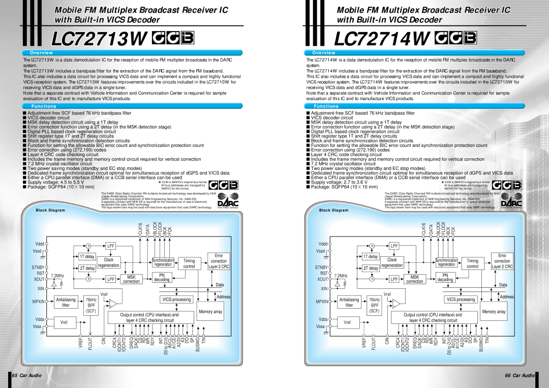
Block Diagram
|
|
|
|
|
|
| CLK16 | DATA | BLOCK FLOCK BCK FCK |
|
|
|
| |
Vddd |
|
|
|
| LPF |
|
|
|
|
|
|
|
|
|
Vssd |
|
|
|
|
|
|
|
|
|
|
|
|
| |
|
|
|
|
|
|
|
|
|
|
|
|
| Error | |
|
| 1T delay | Clock |
|
|
| Synchronization |
| Timing |
| ||||
|
|
|
|
|
|
|
|
| correction | |||||
STNBY |
| 2T delay | regeneration |
|
|
| regeneration |
| control |
| Layer 2 CRC | |||
|
|
|
|
|
|
| ||||||||
RST | 7.2MHz |
|
|
|
|
| MSK |
|
| PN |
|
|
|
|
XOUT |
|
|
| LPF |
|
|
|
|
|
|
| |||
|
|
|
|
|
|
| decoding |
|
|
|
| |||
|
|
|
| correction |
|
|
|
|
|
| ||||
|
|
|
|
|
|
|
|
|
|
|
| Data | ||
XIN |
|
|
|
|
|
|
|
|
|
|
|
|
| |
|
|
|
|
|
|
|
|
|
|
|
|
|
| |
|
|
|
| Vref |
|
|
|
|
| VICS processing |
| Address | ||
MPXIN | Antialiasing |
| 76kHz |
|
|
|
|
|
|
| ||||
|
|
|
|
|
|
|
|
| ||||||
filter |
| BPF |
|
|
|
|
|
|
|
|
|
|
| |
|
|
|
|
|
|
|
|
|
|
|
|
| ||
|
|
| (SCF) |
|
| Output control (CPU interface) and |
| Memory array | ||||||
Vdda |
|
|
|
|
|
|
|
| ||||||
Vref |
|
|
|
|
| layer 4 CRC checking circuit |
|
|
|
| ||||
Vssa |
|
|
|
|
|
|
|
|
|
|
|
|
| |
|
|
|
|
|
|
|
|
|
|
|
|
|
| |
|
| VREF | FLOUT | CIN | CRC4 | IOCNT1 IOCNT2 | DREQ DACK CS RD WR RDY | INT D0 to D15 A0/CL A1/CE | A2/DI | A3 DO SP | BUSWD | TIN | ||
Mobile FM Multiplexultiplex BroadcastBroadcast ReceiverReceiver ICIC with
LC72714W14W 


Overview
The LC72714W is a data demodulation IC for the reception of mobile FM multiplex broadcasts in the DARC system.
The LC72714W includes a bandpass filter for the extraction of the DARC signal from the FM baseband.
This IC also includes a data circuit for processing VICS data and can implement a compact and highly functional VICS reception system. The LC72714W features improvements over the circuits included in the LC72710W for receiving VICS data and dGPS data in a single tuner.
Note that a separate contract with Vehicle Information and Communication Center is required for sample evaluation of this IC and to manufacture VICS products.
Functions
■
■VICS decoder circuit
■MSK delay detection circuit using a 1T delay
■Error correction function using a 2T delay (in the MSK detection stage)
■Digital PLL based clock regeneration circuit
■Shift register type 1T and 2T delay circuits
■Block and frame synchronization detection circuits
■Function for setting the allowable BIC error count and synchronization protection count
■Error correction using (272,190) codes
■Layer 4 CRC code checking circuit
■Includes the frame memory and memory control circuit required for vertical correction
■7.2 MHz crystal oscillator circuit
■Two power saving modes (standby and EC stop modes)
■Dedicated frame synchronization circuit optimal for simultaneous reception of dGPS and VICS data
■Either a CPU parallel interface (DMA) or a CCB serial interface can be used
■ Supply voltage: 2.7 to 3.6 V
■ Package: SQFP64 (10 ![]() 10 mm)
10 mm)
The DARC (Data Radio Channel) FM multiplex broadcast technology was developed by NHK
(Japan Broadcasting Corporation). DARC is a registered trademark of NHK Engineering Services, Inc.
A separate contract with
The logo shown here may be used with electronic equipment that uses DARC technology.
Block Diagram
|
|
|
|
|
|
| CLK16 | DATA | BLOCK FLOCK BCK FCK |
|
|
|
| |
Vddd |
|
|
|
| LPF |
|
|
|
|
|
|
|
|
|
Vssd |
|
|
|
|
|
|
|
|
|
|
|
|
| |
|
|
|
|
|
|
|
|
|
|
|
|
| Error | |
|
| 1T delay | Clock |
|
|
| Synchronization |
| Timing |
| ||||
|
|
|
|
|
|
|
|
| correction | |||||
STNBY |
| 2T delay | regeneration |
|
|
| regeneration |
| control |
| Layer 2 CRC | |||
|
|
|
|
|
|
| ||||||||
RST | 7.2MHz |
|
|
|
|
| MSK |
|
| PN |
|
|
|
|
XOUT |
|
|
| LPF |
|
|
|
|
|
|
| |||
|
|
|
|
|
|
| decoding |
|
|
|
| |||
|
|
|
| correction |
|
|
|
|
|
| ||||
|
|
|
|
|
|
|
|
|
|
|
| Data | ||
XIN |
|
|
|
|
|
|
|
|
|
|
|
|
| |
|
|
|
|
|
|
|
|
|
|
|
|
|
| |
|
|
|
| Vref |
|
|
|
|
| VICS processing |
| Address | ||
MPXIN | Antialiasing |
| 76kHz |
|
|
|
|
|
|
| ||||
|
|
|
|
|
|
|
|
| ||||||
filter |
| BPF |
|
|
|
|
|
|
|
|
|
|
| |
|
|
|
|
|
|
|
|
|
|
|
|
| ||
|
|
| (SCF) |
|
| Output control (CPU interface) and |
| Memory array | ||||||
Vdda |
|
|
|
|
|
|
|
| ||||||
Vref |
|
|
|
|
| layer 4 CRC checking circuit |
|
|
|
| ||||
Vssa |
|
|
|
|
|
|
|
|
|
|
|
|
| |
|
|
|
|
|
|
|
|
|
|
|
|
|
| |
|
| VREF | FLOUT | CIN | CRC4 | IOCNT1 IOCNT2 | DREQ DACK CS RD WR RDY | INT D0 to D15 A0/CL A1/CE | A2/DI | A3 DO SP | BUSWD | TIN | ||
| 65 Car Audio | 66 Car Audio |
|
|
|