NW-A805/A806/A808/NWZ-A815/A816/A818
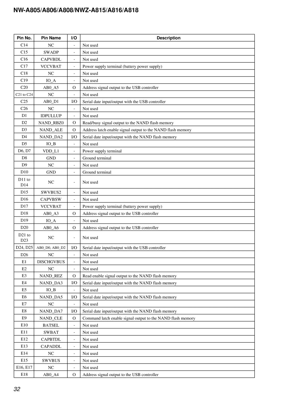
Pin No. | Pin Name | I/O | Description | |
|
|
|
| |
C14 | NC | - | Not used | |
|
|
|
| |
C15 | SWADP | - | Not used | |
|
|
|
| |
C16 | CAPVBDL | - | Not used | |
|
|
|
| |
C17 | VCCVBAT | - | Power supply terminal (battery power supply) | |
C18 | NC | - | Not used | |
C19 | IO_A | - | Not used | |
C20 | AB0_A5 | O | Address signal output to the USB controller | |
|
|
|
| |
C21 to C24 | NC | - | Not used | |
|
|
|
| |
C25 | AB0_D1 | I/O | Serial date input/output with the USB controller | |
|
|
|
| |
C26 | NC | - | Not used | |
D1 | IDPULLUP | - | Not used | |
D2 | NAND_RBZ0 | O | Read/busy signal output to the NAND flash memory | |
D3 | NAND_ALE | O | Address latch enable signal output to the NAND flash memory | |
|
|
|
| |
D4 | NAND_DA2 | I/O | Serial date input/output with the NAND flash memory | |
|
|
|
| |
D5 | IO_B | - | Not used | |
|
|
|
| |
D6, D7 | VDD_L1 | - | Power supply terminal | |
D8 | GND | - | Ground terminal | |
D9 | NC | - | Not used | |
D10 | GND | - | Ground terminal | |
|
|
|
| |
D11 to | NC | - | Not used | |
D14 | ||||
|
|
| ||
|
|
|
| |
D15 | SWVBUS2 | - | Not used | |
|
|
|
| |
D16 | CAPVBSW | - | Not used | |
D17 | VCCVBAT | - | Power supply terminal (battery power supply) | |
D18 | AB0_A3 | O | Address signal output to the USB controller | |
D19 | IO_A | - | Not used | |
|
|
|
| |
D20 | AB0_A6 | O | Address signal output to the USB controller | |
|
|
|
| |
D21 to | NC | - | Not used | |
D23 | ||||
|
|
| ||
|
|
|
| |
D24, D25 | AB0_D0, AB0_D2 | I/O | Serial date input/output with the USB controller | |
D26 | NC | - | Not used | |
E1 | DISCHGVBUS | - | Not used | |
E2 | NC | - | Not used | |
|
|
|
| |
E3 | NAND_REZ | O | Read enable signal output to the NAND flash memory | |
|
|
|
| |
E4 | NAND_DA3 | I/O | Serial date input/output with the NAND flash memory | |
|
|
|
| |
E5 | IO_B | - | Not used | |
|
|
|
| |
E6 | NAND_DA5 | I/O | Serial date input/output with the NAND flash memory | |
E7 | NC | - | Not used | |
E8 | NAND_DA7 | I/O | Serial date input/output with the NAND flash memory | |
|
|
|
| |
E9 | NAND_CLE | O | Command latch enable signal output to the NAND flash memory | |
|
|
|
| |
E10 | BATSEL | - | Not used | |
|
|
|
| |
E11 | SWBAT | - | Not used | |
|
|
|
| |
E12 | CAPBTDL | - | Not used | |
E13 | CAPADDL | - | Not used | |
E14 | NC | - | Not used | |
E15 | SWVBUS | - | Not used | |
|
|
|
| |
E16, E17 | NC | - | Not used | |
|
|
|
| |
E18 | AB0_A4 | O | Address signal output to the USB controller | |
|
|
|
|
32