NW-A805/A806/A808/NWZ-A815/A816/A818
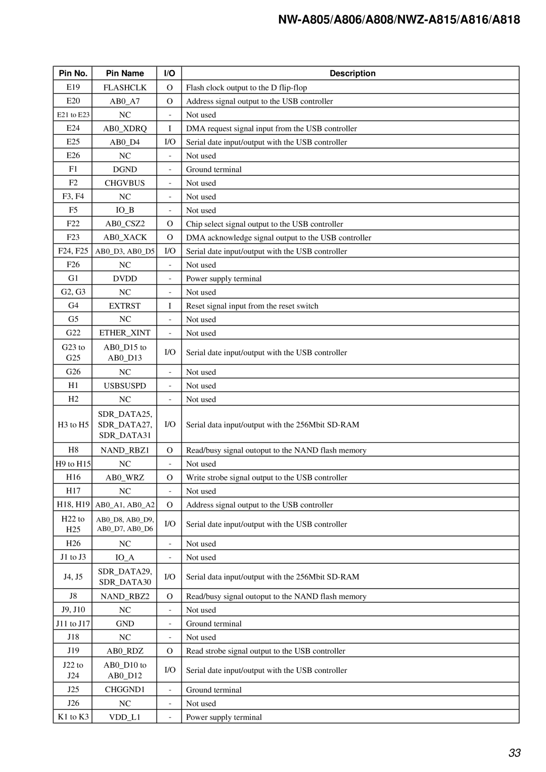
Pin No. | Pin Name | I/O | Description | |
|
|
|
| |
E19 | FLASHCLK | O | Flash clock output to the D | |
|
|
|
| |
E20 | AB0_A7 | O | Address signal output to the USB controller | |
|
|
|
| |
E21 to E23 | NC | - | Not used | |
|
|
|
| |
E24 | AB0_XDRQ | I | DMA request signal input from the USB controller | |
E25 | AB0_D4 | I/O | Serial date input/output with the USB controller | |
E26 | NC | - | Not used | |
|
|
|
| |
F1 | DGND | - | Ground terminal | |
|
|
|
| |
F2 | CHGVBUS | - | Not used | |
|
|
|
| |
F3, F4 | NC | - | Not used | |
|
|
|
| |
F5 | IO_B | - | Not used | |
F22 | AB0_CSZ2 | O | Chip select signal output to the USB controller | |
F23 | AB0_XACK | O | DMA acknowledge signal output to the USB controller | |
F24, F25 | AB0_D3, AB0_D5 | I/O | Serial date input/output with the USB controller | |
|
|
|
| |
F26 | NC | - | Not used | |
|
|
|
| |
G1 | DVDD | - | Power supply terminal | |
|
|
|
| |
G2, G3 | NC | - | Not used | |
G4 | EXTRST | I | Reset signal input from the reset switch | |
G5 | NC | - | Not used | |
G22 | ETHER_XINT | - | Not used | |
|
|
|
| |
G23 to | AB0_D15 to | I/O | Serial date input/output with the USB controller | |
G25 | AB0_D13 | |||
|
| |||
|
|
|
| |
G26 | NC | - | Not used | |
|
|
|
| |
H1 | USBSUSPD | - | Not used | |
H2 | NC | - | Not used | |
| SDR_DATA25, |
|
| |
H3 to H5 | SDR_DATA27, | I/O | Serial data input/output with the 256Mbit | |
| SDR_DATA31 |
|
| |
|
|
|
| |
H8 | NAND_RBZ1 | O | Read/busy signal outoput to the NAND flash memory | |
H9 to H15 | NC | - | Not used | |
H16 | AB0_WRZ | O | Write strobe signal output to the USB controller | |
|
|
|
| |
H17 | NC | - | Not used | |
|
|
|
| |
H18, H19 | AB0_A1, AB0_A2 | O | Address signal output to the USB controller | |
|
|
|
| |
H22 to | AB0_D8, AB0_D9, | I/O | Serial date input/output with the USB controller | |
H25 | AB0_D7, AB0_D6 | |||
|
| |||
|
|
|
| |
H26 | NC | - | Not used | |
J1 to J3 | IO_A | - | Not used | |
|
|
|
| |
J4, J5 | SDR_DATA29, | I/O | Serial data input/output with the 256Mbit | |
SDR_DATA30 | ||||
|
|
| ||
|
|
|
| |
J8 | NAND_RBZ2 | O | Read/busy signal outoput to the NAND flash memory | |
|
|
|
| |
J9, J10 | NC | - | Not used | |
|
|
|
| |
J11 to J17 | GND | - | Ground terminal | |
J18 | NC | - | Not used | |
J19 | AB0_RDZ | O | Read strobe signal output to the USB controller | |
|
|
|
| |
J22 to | AB0_D10 to | I/O | Serial date input/output with the USB controller | |
J24 | AB0_D12 | |||
|
| |||
|
|
|
| |
J25 | CHGGND1 | - | Ground terminal | |
|
|
|
| |
J26 | NC | - | Not used | |
|
|
|
| |
K1 to K3 | VDD_L1 | - | Power supply terminal |
33