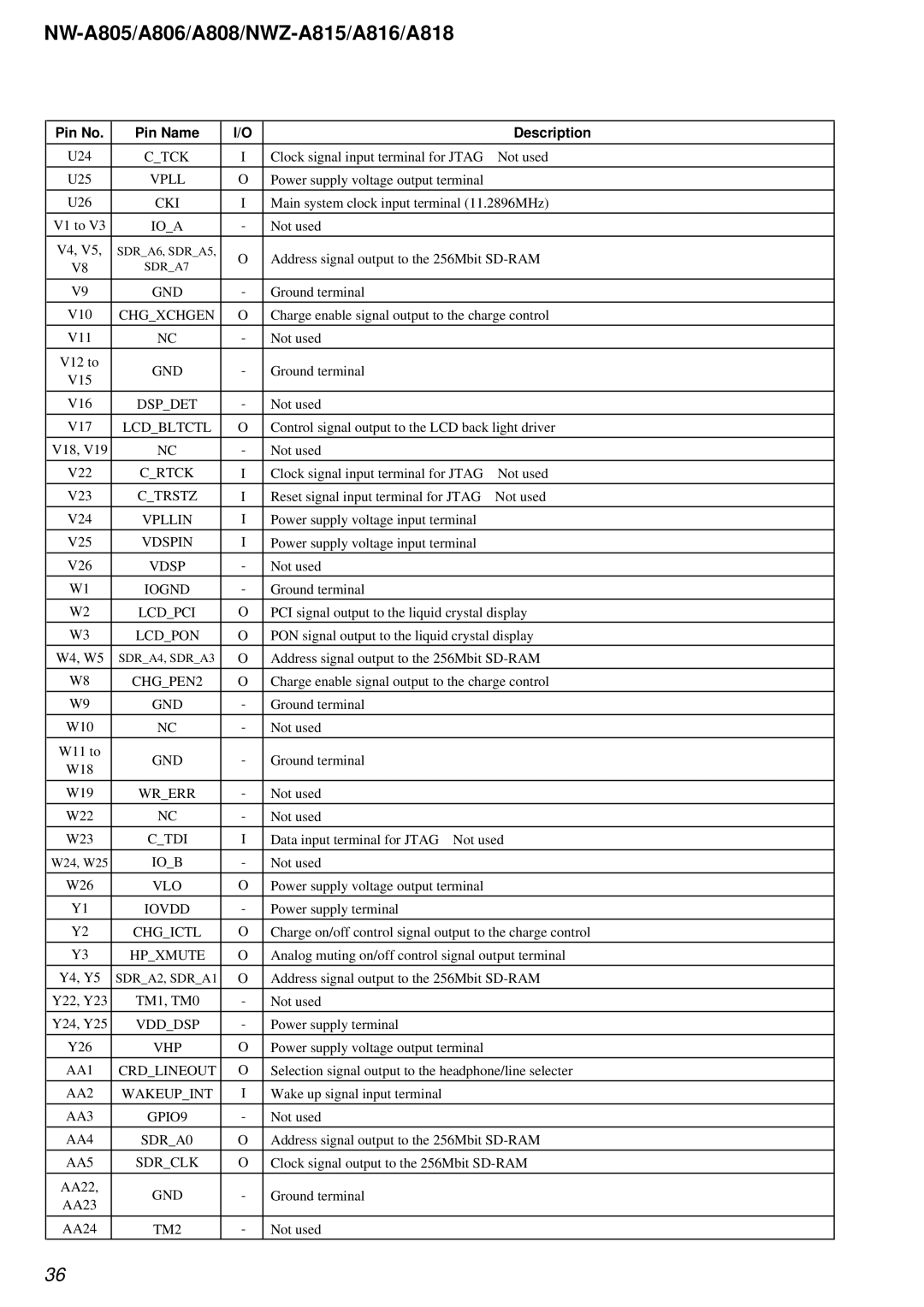
NW-A805/A806/A808/NWZ-A815/A816/A818
Pin No. | Pin Name | I/O |
| Description | |
|
|
|
|
| |
U24 | C_TCK | I | Clock signal input terminal for JTAG | Not used | |
U25 | VPLL | O | Power supply voltage output terminal |
| |
|
|
|
| ||
U26 | CKI | I | Main system clock input terminal (11.2896MHz) | ||
|
|
|
|
| |
V1 to V3 | IO_A | - | Not used |
| |
|
|
|
|
| |
V4, V5, | SDR_A6, SDR_A5, | O | Address signal output to the 256Mbit | ||
V8 | SDR_A7 | ||||
|
|
| |||
|
|
|
|
| |
V9 | GND | - | Ground terminal |
| |
V10 | CHG_XCHGEN | O | Charge enable signal output to the charge control | ||
V11 | NC | - | Not used |
| |
V12 to | GND | - | Ground terminal |
| |
V15 |
| ||||
|
|
|
| ||
|
|
|
|
| |
V16 | DSP_DET | - | Not used |
| |
|
|
|
| ||
V17 | LCD_BLTCTL | O | Control signal output to the LCD back light driver | ||
|
|
|
|
| |
V18, V19 | NC | - | Not used |
| |
V22 | C_RTCK | I | Clock signal input terminal for JTAG | Not used | |
V23 | C_TRSTZ | I | Reset signal input terminal for JTAG | Not used | |
V24 | VPLLIN | I | Power supply voltage input terminal |
| |
|
|
|
|
| |
V25 | VDSPIN | I | Power supply voltage input terminal |
| |
|
|
|
|
| |
V26 | VDSP | - | Not used |
| |
|
|
|
|
| |
W1 | IOGND | - | Ground terminal |
| |
W2 | LCD_PCI | O | PCI signal output to the liquid crystal display | ||
W3 | LCD_PON | O | PON signal output to the liquid crystal display | ||
W4, W5 | SDR_A4, SDR_A3 | O | Address signal output to the 256Mbit | ||
|
|
|
| ||
W8 | CHG_PEN2 | O | Charge enable signal output to the charge control | ||
|
|
|
|
| |
W9 | GND | - | Ground terminal |
| |
|
|
|
|
| |
W10 | NC | - | Not used |
| |
|
|
|
|
| |
W11 to | GND | - | Ground terminal |
| |
W18 |
| ||||
|
|
|
| ||
|
|
|
|
| |
W19 | WR_ERR | - | Not used |
| |
W22 | NC | - | Not used |
| |
|
|
|
| ||
W23 | C_TDI | I | Data input terminal for JTAG Not used | ||
|
|
|
|
| |
W24, W25 | IO_B | - | Not used |
| |
|
|
|
|
| |
W26 | VLO | O | Power supply voltage output terminal |
| |
|
|
|
|
| |
Y1 | IOVDD | - | Power supply terminal |
| |
Y2 | CHG_ICTL | O | Charge on/off control signal output to the charge control | ||
Y3 | HP_XMUTE | O | Analog muting on/off control signal output terminal | ||
|
|
|
| ||
Y4, Y5 | SDR_A2, SDR_A1 | O | Address signal output to the 256Mbit | ||
|
|
|
|
| |
Y22, Y23 | TM1, TM0 | - | Not used |
| |
|
|
|
|
| |
Y24, Y25 | VDD_DSP | - | Power supply terminal |
| |
|
|
|
|
| |
Y26 | VHP | O | Power supply voltage output terminal |
| |
AA1 | CRD_LINEOUT | O | Selection signal output to the headphone/line selecter | ||
AA2 | WAKEUP_INT | I | Wake up signal input terminal |
| |
|
|
|
|
| |
AA3 | GPIO9 | - | Not used |
| |
|
|
|
| ||
AA4 | SDR_A0 | O | Address signal output to the 256Mbit | ||
|
|
|
| ||
AA5 | SDR_CLK | O | Clock signal output to the 256Mbit | ||
|
|
|
|
| |
AA22, | GND | - | Ground terminal |
| |
AA23 |
| ||||
|
|
|
| ||
|
|
|
|
| |
AA24 | TM2 | - | Not used |
| |
36