NW-A805/A806/A808/NWZ-A815/A816/A818
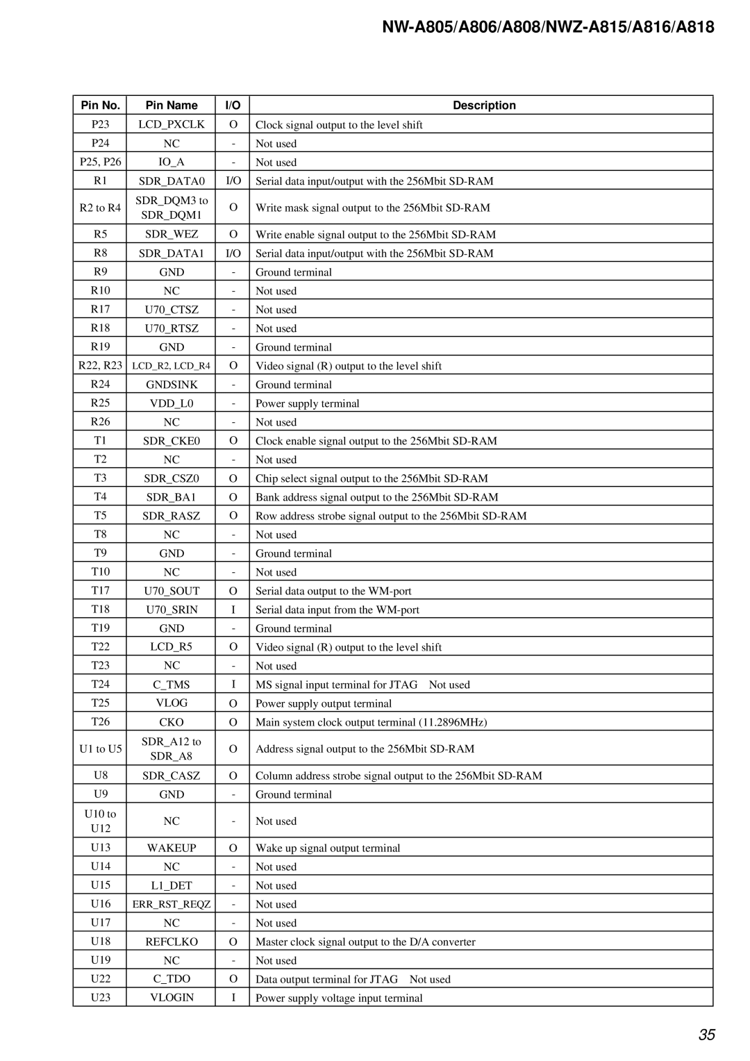
Pin No. | Pin Name | I/O | Description | |
|
|
|
| |
P23 | LCD_PXCLK | O | Clock signal output to the level shift | |
|
|
|
| |
P24 | NC | - | Not used | |
P25, P26 | IO_A | - | Not used | |
R1 | SDR_DATA0 | I/O | Serial data input/output with the 256Mbit | |
|
|
|
| |
R2 to R4 | SDR_DQM3 to | O | Write mask signal output to the 256Mbit | |
SDR_DQM1 | ||||
|
|
| ||
|
|
|
| |
R5 | SDR_WEZ | O | Write enable signal output to the 256Mbit | |
|
|
|
| |
R8 | SDR_DATA1 | I/O | Serial data input/output with the 256Mbit | |
|
|
|
| |
R9 | GND | - | Ground terminal | |
R10 | NC | - | Not used | |
R17 | U70_CTSZ | - | Not used | |
R18 | U70_RTSZ | - | Not used | |
|
|
|
| |
R19 | GND | - | Ground terminal | |
|
|
|
| |
R22, R23 | LCD_R2, LCD_R4 | O | Video signal (R) output to the level shift | |
|
|
|
| |
R24 | GNDSINK | - | Ground terminal | |
R25 | VDD_L0 | - | Power supply terminal | |
R26 | NC | - | Not used | |
T1 | SDR_CKE0 | O | Clock enable signal output to the 256Mbit | |
|
|
|
| |
T2 | NC | - | Not used | |
|
|
|
| |
T3 | SDR_CSZ0 | O | Chip select signal output to the 256Mbit | |
|
|
|
| |
T4 | SDR_BA1 | O | Bank address signal output to the 256Mbit | |
T5 | SDR_RASZ | O | Row address strobe signal output to the 256Mbit | |
T8 | NC | - | Not used | |
T9 | GND | - | Ground terminal | |
|
|
|
| |
T10 | NC | - | Not used | |
|
|
|
| |
T17 | U70_SOUT | O | Serial data output to the | |
|
|
|
| |
T18 | U70_SRIN | I | Serial data input from the | |
|
|
|
| |
T19 | GND | - | Ground terminal | |
T22 | LCD_R5 | O | Video signal (R) output to the level shift | |
T23 | NC | - | Not used | |
T24 | C_TMS | I | MS signal input terminal for JTAG Not used | |
|
|
|
| |
T25 | VLOG | O | Power supply output terminal | |
|
|
|
| |
T26 | CKO | O | Main system clock output terminal (11.2896MHz) | |
|
|
|
| |
U1 to U5 | SDR_A12 to | O | Address signal output to the 256Mbit | |
SDR_A8 | ||||
|
|
| ||
|
|
|
| |
U8 | SDR_CASZ | O | Column address strobe signal output to the 256Mbit | |
U9 | GND | - | Ground terminal | |
U10 to | NC | - | Not used | |
U12 | ||||
|
|
| ||
|
|
|
| |
U13 | WAKEUP | O | Wake up signal output terminal | |
|
|
|
| |
U14 | NC | - | Not used | |
|
|
|
| |
U15 | L1_DET | - | Not used | |
U16 | ERR_RST_REQZ | - | Not used | |
U17 | NC | - | Not used | |
|
|
|
| |
U18 | REFCLKO | O | Master clock signal output to the D/A converter | |
|
|
|
| |
U19 | NC | - | Not used | |
|
|
|
| |
U22 | C_TDO | O | Data output terminal for JTAG Not used | |
|
|
|
| |
U23 | VLOGIN | I | Power supply voltage input terminal |
35