![]()
![]()
![]()
![]()
![]()
![]()
![]()
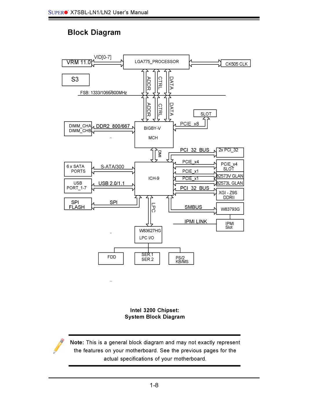
Block Diagram
VRM 11.0
S3
FSB: 1333/1066/800MHz
LGA775_PROCESSOR
ADDR | CTRL | DATA |
CK505 CLK
DIMM_CHA DIMM_CHB
6 x SATA PORTS
USB
DDR2_800/667
3
USB 2.0/1.1
ADDR | CTRL |
MCH
![]() DMI
DMI
DATA
SLOT
PCIE_x8
PCI_32_BUS
PCIE_x4
PCIE_x1
PCIE_x1
PCI_32_BUS
2x PCI_32
PCIE_x4
SLOT
82573V GLAN
82573L GLAN
XGI - Z9S
DDRII
SPI
FLASH
SPI
LPC
W83627HG
SMBUS | W83793G | ||
| |||
IPMI LINK |
|
| |
|
| ||
IPMI | |||
| |||
| Slot | ||
|
|
| |
4
FDD
LPC I/O
|
|
|
|
|
|
|
|
|
|
|
|
SER.1 |
|
| PS/2 | ||
SER.2 |
|
| |||
|
| KB/MS | |||
|
|
|
| ||
Intel 3200 Chipset:
System Block Diagram
Note: This is a general block diagram and may not exactly represent the features on your motherboard. See the previous pages for the actual specifi cations of your motherboard.