GE863-QUAD
1vv0300715 Rev. 1 - 19/09/06
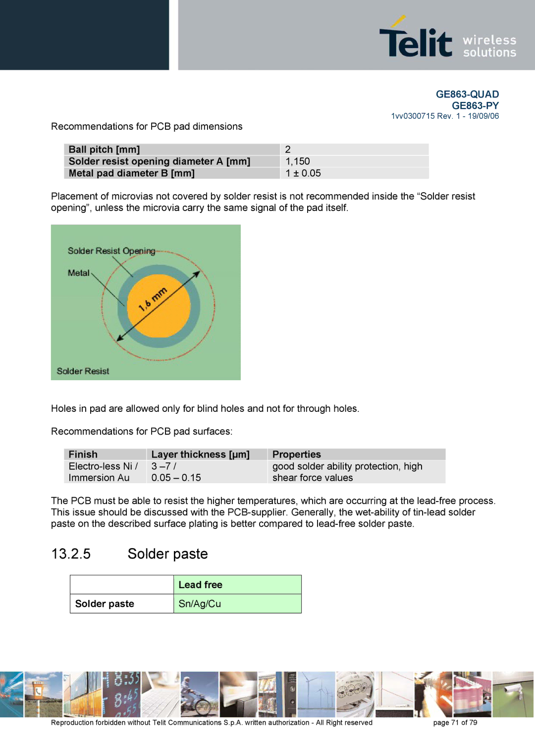
Recommendations for PCB pad dimensions |
|
| |
|
|
|
|
| Ball pitch [mm] | 2 | |
| Solder resist opening diameter A [mm] |
| 1,150 |
| Metal pad diameter B [mm] |
| 1 ± 0.05 |
Placement of microvias not covered by solder resist is not recommended inside the “Solder resist opening”, unless the microvia carry the same signal of the pad itself.
Holes in pad are allowed only for blind holes and not for through holes.
Recommendations for PCB pad surfaces:
Finish | Layer thickness [µm] | Properties |
3 | good solder ability protection, high | |
Immersion Au | 0.05 – 0.15 | shear force values |
The PCB must be able to resist the higher temperatures, which are occurring at the
13.2.5Solder paste
| Lead free |
|
|
Solder paste | Sn/Ag/Cu |
|
|
Reproduction forbidden without Telit Communications S.p.A. written authorization - All Right reserved | page 71 of 79 |