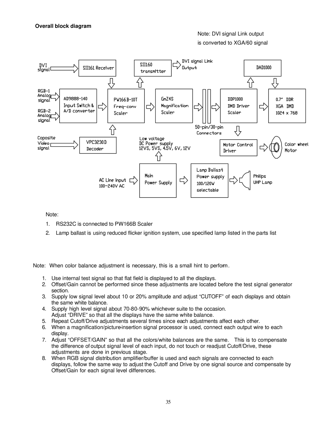
Overall block diagram
Note: DVI signal Link output
is converted to XGA/60 signal
Note:
1.RS232C is connected to PW166B Scaler
2.Lamp ballast is using reduced flicker ignition system, use specified lamp listed in the parts list
Note: When color balance adjustment is necessary, this is a small hint to perform .
1.Use internal test signal so that flat field is displayed to all the displays.
2.Offset/Gain cannot be performed since these adjustments are located before the test signal generator section.
3.Supply low signal level about 10 or 20% amplitude and adjust “CUTOFF” of each displays and obtain the same white balance.
4.Supply high level signal about
5.Repeat Cutoff/Drive adjustments several times since each adjustments affect each other.
6.When a
7.Adjust “OFFSET/GAIN” so that all the colors/white balances are the same. This is to compensate the difference of output signal level of each input, do not touch or readjust Cutoff/Drive, these adjustments are done in previous stage.
8.When RGB signal distribution amplifier/buffer is used and each signals are connected to each displays, follow the same way to adjust the Cutoff and Drive by one signal source and compensate by Offset/Gain for each signal level differences.
35