VXI Technology, Inc.
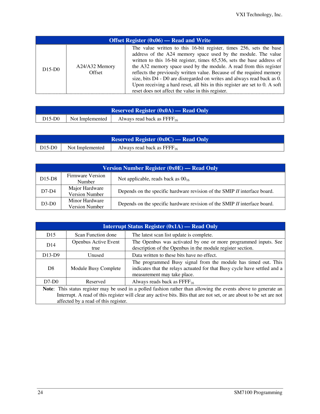
Offset Register (0x06) — Read and Write
A24/A32 Memory
Offset
The value written to this
Reserved Register (0x0A) — Read Only
Not Implemented
Always read back as FFFF16
Reserved Register (0x0C) — Read Only
Not Implemented
Always read back as FFFF16
|
| Version Number Register (0x0E) — Read Only | |
| Firmware Version | Not applicable, reads back as 0016 | |
| Number | ||
|
|
| |
| Major Hardware | Depends on the specific hardware revision of the SMIP II interface board. | |
| Version Number | ||
|
|
| |
| Minor Hardware | Depends on the specific hardware revision of the SMIP II interface board. | |
| Version Number | ||
|
|
| |
Interrupt Status Register (0x1A) — Read Only
D15 | Scan Function done | The latest scan list update is complete. | |
D14 | Openbus Active Event | The Openbus was activated by one or more programmed inputs. See | |
true | description of the Openbus in the module register section. | ||
| |||
Unused | Data written to these bits have no effect. | ||
|
| The programmed Busy signal from the module has timed out. This | |
D8 | Module Busy Complete | indicates that the relays actuated for that Busy cycle have settled and a | |
|
| measurement may take place. | |
Reserved | Always reads back as FFFF16 |
Note: This status register may be used in a polled fashion rather than allowing the events above to generate an Interrupt. A read of this register will clear any active bits. Bits that are not set, or are about to be set are not affected by a read of this register.
24 | SM7100 Programming |