www.vxitech.com
DESCRIPTION OF SMIP II MODULE REGISTERS - A24 / A32 - EXTENDED MEMORY
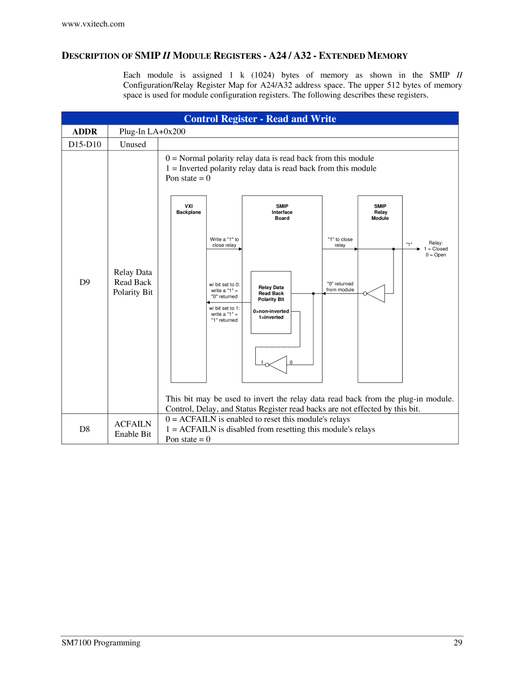
Each module is assigned 1 k (1024) bytes of memory as shown in the SMIP II Configuration/Relay Register Map for A24/A32 address space. The upper 512 bytes of memory space is used for module configuration registers. The following describes these registers.
Control Register - Read and Write
ADDR | |
Unused |
0 = Normal polarity relay data is read back from this module 1 = Inverted polarity relay data is read back from this module Pon state = 0
| VXI |
| SMIP |
|
| SMIP |
|
| Backplane |
| Interface |
| Relay |
| |
|
|
| Board |
|
| Module |
|
|
| Write a "1" to |
|
| "1" to close | "1" | Relay: |
|
| close relay |
|
| relay | ||
|
|
|
|
|
|
| 1 = Closed |
|
|
|
|
|
|
| 0 = Open |
| Relay Data |
|
|
|
|
|
|
D9 | Read Back | w/ bit set to 0: | Relay Data |
| "0" returned |
|
|
| Polarity Bit | write a "1" = |
| from module |
|
| |
| Read Back |
|
|
| |||
| "0" returned |
|
|
|
| ||
|
| Polarity Bit |
|
|
|
| |
|
|
|
|
|
|
| |
|
| w/ bit set to 1: |
|
|
|
| |
|
| write a "1" = |
|
|
|
| |
|
| 1=inverted |
|
|
|
| |
|
| "1" returned |
|
|
|
| |
|
|
|
|
|
|
| |
|
|
| 1 | 0 |
|
|
|
|
| This bit may be used to invert the relay data read back from the | ||
|
| Control, Delay, and Status Register read backs are not effected by this bit. | ||
D8 | ACFAILN | 0 | = ACFAILN is enabled to reset this module's relays | |
1 | = ACFAILN is disabled from resetting this module's relays | |||
Enable Bit | ||||
| Pon state = 0 | |||
|
| |||
SM7100 Programming | 29 |