R
Read Datapath
Controller to Read Datapath Interface
Table 4 lists the control signals between the controller and the read datapath.
Table 4: Signals between Controller and Read Datapath
Signal Name | Signal | Signal Description | Notes | |
Width | ||||
|
|
| ||
|
|
|
| |
ctrl_Dummyread_Start | 1 | Output from the controller to the | This signal must be asserted when valid read data | |
|
| read datapath. When this signal | is available on the data bus. | |
|
| is asserted, the strobe and data | This signal is deasserted when the | |
|
| calibration begin. | ||
|
| dp_dly_slct_done signal is asserted. | ||
|
|
| ||
|
|
|
| |
dp_dly_slct_done | 1 | Output from the read datapath | This signal is asserted when the data and strobe | |
|
| to the controller indicating the | have been calibrated. | |
|
| strobe and data calibration are | Normal operation begins after this signal is | |
|
| complete. | ||
|
| asserted. | ||
|
|
| ||
|
|
|
| |
ctrl_RdEn_div0 | 1 | Output from the controller to the | This signal is asserted for one CLKdiv_0 clock | |
|
| read datapath used as the write | cycle for a burst length of 4 and two clock cycles for | |
|
| enable to the read data capture | a burst length of 8. | |
|
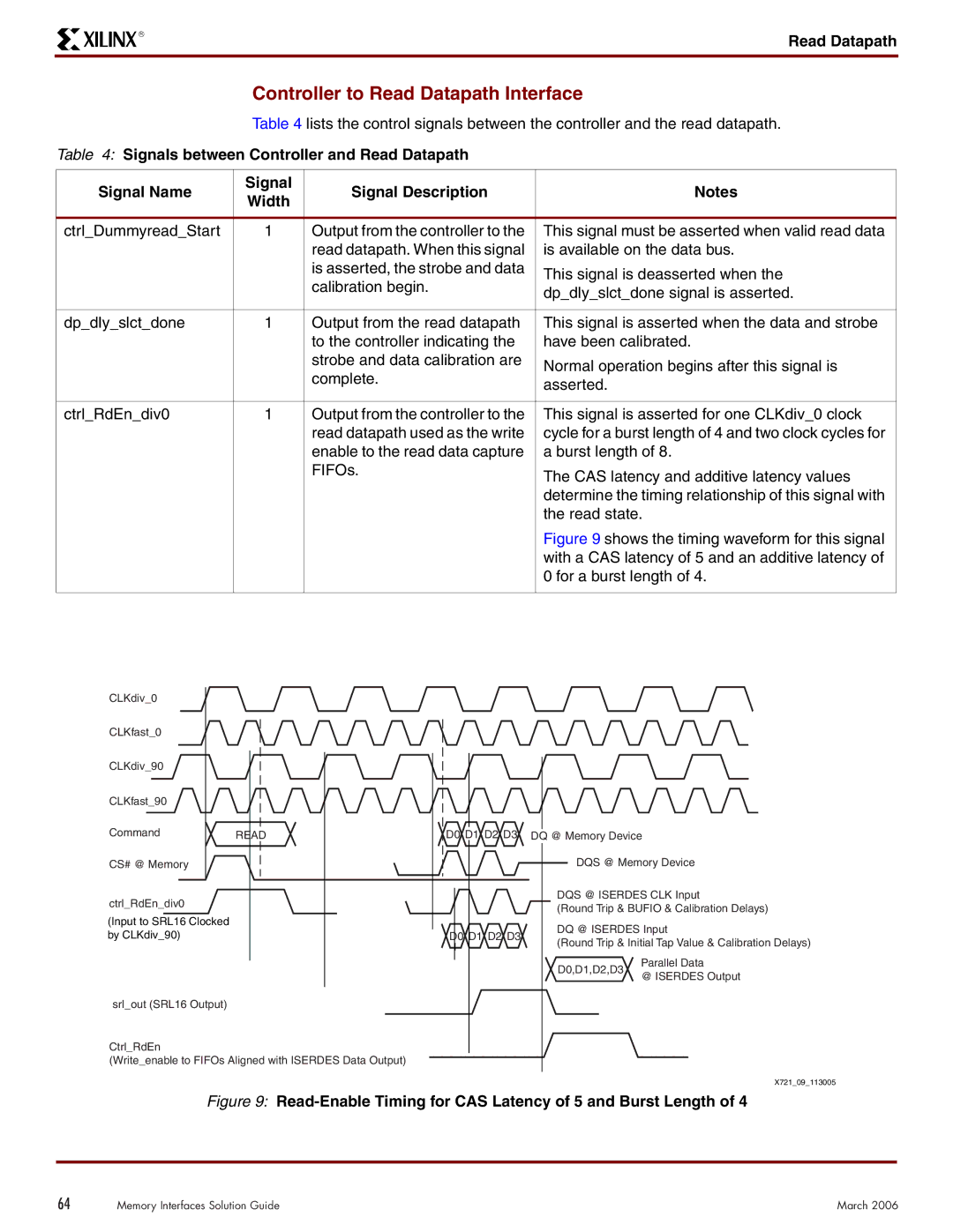
| FIFOs. | The CAS latency and additive latency values | |
|
|
| ||
|
|
| determine the timing relationship of this signal with | |
|
|
| the read state. | |
|
|
| Figure 9 shows the timing waveform for this signal | |
|
|
| with a CAS latency of 5 and an additive latency of | |
|
|
| 0 for a burst length of 4. | |
|
|
|
|
CLKdiv_0
CLKfast_0
CLKdiv_90
CLKfast_90
Command | READ |
CS# @ Memory
ctrl_RdEn_div0
(Input to SRL16 Clocked by CLKdiv_90)
D0 D1 D2 D3 DQ @ Memory Device
DQS @ Memory Device
DQS @ ISERDES CLK Input
(Round Trip & BUFIO & Calibration Delays)
D0 D1 D2 D3 | DQ @ ISERDES Input | |
(Round Trip & Initial Tap Value & Calibration Delays) | ||
|
srl_out (SRL16 Output)
Ctrl_RdEn
(Write_enable to FIFOs Aligned with ISERDES Data Output)
D0,D1,D2,D3
Parallel Data
@ ISERDES Output
X721_09_113005
Figure 9: Read-Enable Timing for CAS Latency of 5 and Burst Length of 4
64 | Memory Interfaces Solution Guide | March 2006 |