R
Reference Design Utilization
Reference
Design
Utilization
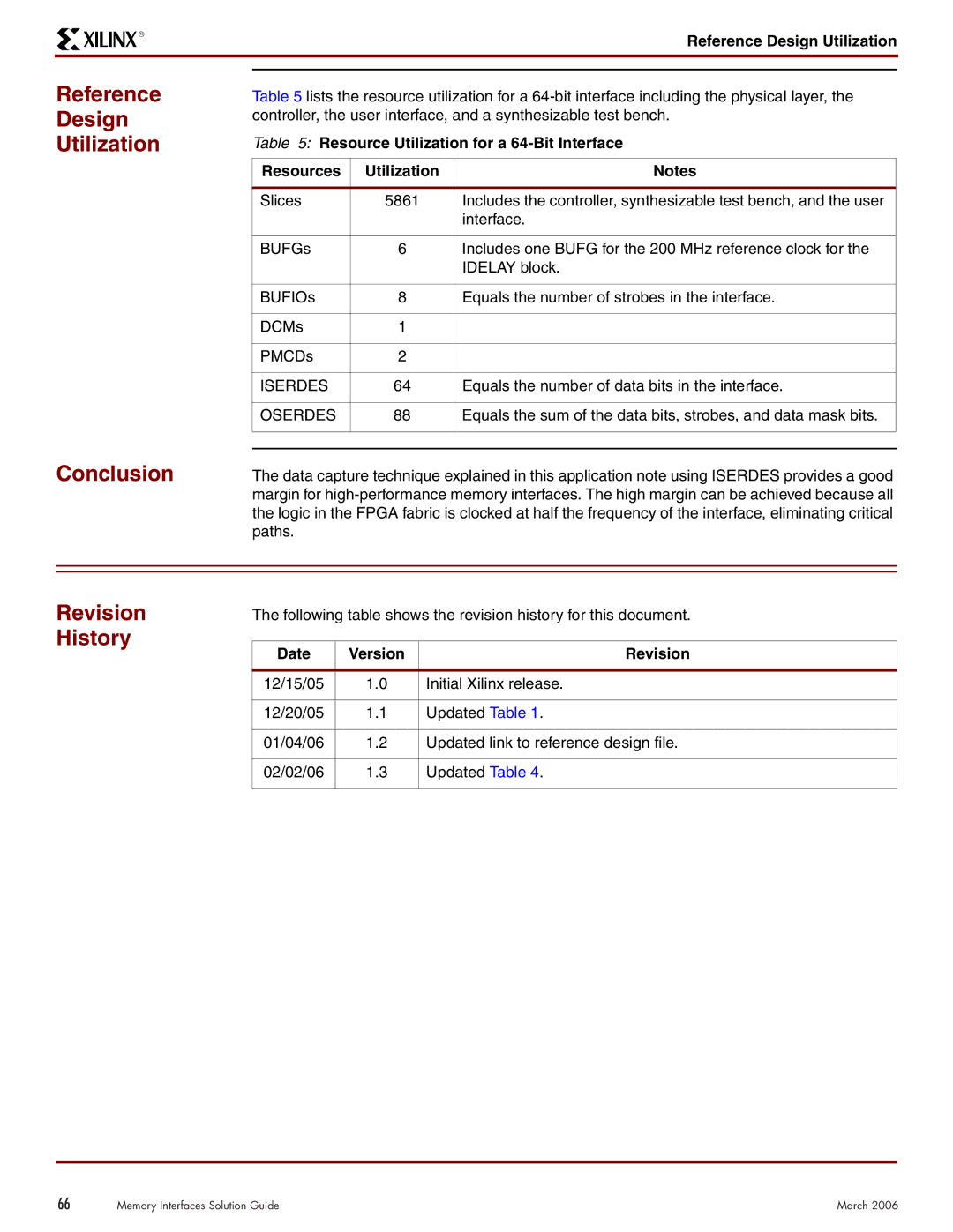
Table 5 lists the resource utilization for a
Table 5: Resource Utilization for a 64-Bit Interface
Resources | Utilization | Notes |
|
|
|
Slices | 5861 | Includes the controller, synthesizable test bench, and the user |
|
| interface. |
|
|
|
BUFGs | 6 | Includes one BUFG for the 200 MHz reference clock for the |
|
| IDELAY block. |
|
|
|
BUFIOs | 8 | Equals the number of strobes in the interface. |
|
|
|
DCMs | 1 |
|
|
|
|
PMCDs | 2 |
|
|
|
|
ISERDES | 64 | Equals the number of data bits in the interface. |
|
|
|
OSERDES | 88 | Equals the sum of the data bits, strobes, and data mask bits. |
|
|
|
|
|
|
Conclusion
The data capture technique explained in this application note using ISERDES provides a good margin for
Revision History
The following table shows the revision history for this document.
Date | Version | Revision |
|
|
|
12/15/05 | 1.0 | Initial Xilinx release. |
|
|
|
12/20/05 | 1.1 | Updated Table 1. |
|
|
|
01/04/06 | 1.2 | Updated link to reference design file. |
|
|
|
02/02/06 | 1.3 | Updated Table 4. |
|
|
|
66 | Memory Interfaces Solution Guide | March 2006 |