R
Write Datapath
DCM |
| PMCD#1 | ||
CLKfast Input | CLK0 |
| CLKA | CLKfast_0 |
CLKIN |
| CLKA1 | ||
System Reset* | CLK90 | * | RST | CLKdiv_0 |
RST | ||||
|
|
|
| CLKA1D2 |
CLKFB | LOCKED |
| CLKFB |
|
PMCD#2
CLKfast_90
![]() CLKA CLKA1
CLKA CLKA1
![]() CLKB
CLKB
CLKdiv_90
* ![]() RST CLKA1D2
RST CLKA1D2
![]() CLKFB
CLKFB
x702_04_051105
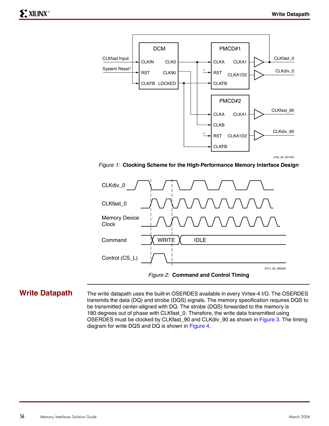
Figure 1: Clocking Scheme for the High-Performance Memory Interface Design
CLKdiv_0
CLKfast_0
Memory Device
Clock
Command | WRITE | IDLE |
Control (CS_L)
X721_02_080205
Figure 2: Command and Control Timing
Write Datapath The write datapath uses the
180 degrees out of phase with CLKfast_0. Therefore, the write data transmitted using OSERDES must be clocked by CLKfast_90 and CLKdiv_90 as shown in Figure 3. The timing diagram for write DQS and DQ is shown in Figure 4.
56 | Memory Interfaces Solution Guide | March 2006 |