R
Read Datapath
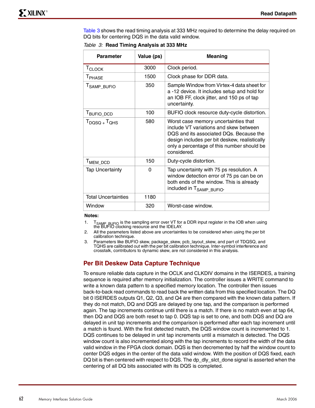
Table 3 shows the read timing analysis at 333 MHz required to determine the delay required on DQ bits for centering DQS in the data valid window.
Table 3: Read Timing Analysis at 333 MHz
Parameter | Value (ps) | Meaning |
|
|
|
TCLOCK | 3000 | Clock period. |
TPHASE | 1500 | Clock phase for DDR data. |
TSAMP_BUFIO | 350 | Sample Window from |
|
| a |
|
| an IOB FF, clock jitter, and 150 ps of tap |
|
| uncertainty. |
|
|
|
TBUFIO_DCD | 100 | BUFIO clock resource |
TDQSQ + TQHS | 580 | Worst case memory uncertainties that |
|
| include VT variations and skew between |
|
| DQS and its associated DQs. Because the |
|
| design includes per bit deskew, realistically |
|
| only a percentage of this number should be |
|
| considered. |
|
|
|
TMEM_DCD | 150 | |
Tap Uncertainty | 0 | Tap uncertainty with 75 ps resolution. A |
|
| window detection error of 75 ps can be on |
|
| both ends of the window. This is already |
|
| included in TSAMP_BUFIO. |
Total Uncertainties | 1180 |
|
|
|
|
Window | 320 | |
|
|
|
Notes:
1.TSAMP_BUFIO is the sampling error over VT for a DDR input register in the IOB when using the BUFIO clocking resource and the IDELAY.
2.All the parameters listed above are uncertainties to be considered when using the per bit calibration technique.
3.Parameters like BUFIO skew, package_skew, pcb_layout_skew, and part of TDQSQ, and TQHS are calibrated out with the per bit calibration technique.
Per Bit Deskew Data Capture Technique
To ensure reliable data capture in the OCLK and CLKDIV domains in the ISERDES, a training sequence is required after memory initialization. The controller issues a WRITE command to write a known data pattern to a specified memory location. The controller then issues
62 | Memory Interfaces Solution Guide | March 2006 |