R
Write Datapath
CLKdiv_0
Clock Forwarded to Memory Device
CLKdiv_90
CLKfast_90 |
|
|
|
Command | WRITE |
| IDLE |
|
| ||
Control (CS_L) |
|
|
|
ctrl_WrEn |
|
|
|
ctrl_wr_disable |
|
|
|
User Interface Data | D0,D1,D2,D3 |
|
|
FIFO Out |
|
| |
|
|
| |
OSERDES Inputs D1, D2, D3, D4 |
| X,X,D0,D1 | D2,D3,X,X |
OSERDES Inputs T1, T2, T3, T4 |
| 1,1,0,0 | 0,0,1,1 |
Strobe (DQS) |
|
|
|
Data (DQ), OSERDES Output |
|
| D0 D1 D2 D3 |
X721_05_080205
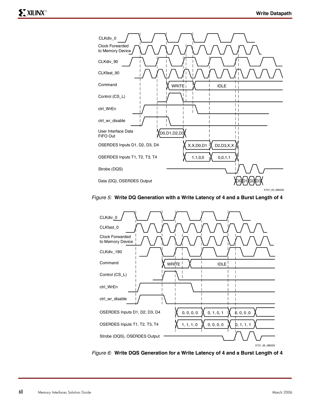
Figure 5: Write DQ Generation with a Write Latency of 4 and a Burst Length of 4
CLKdiv_0
CLKfast_0
Clock Forwarded to Memory Device
CLKdiv_180
Command
Control (CS_L)
ctrl_WrEn
ctrl_wr_disable
OSERDES Inputs D1, D2, D3, D4
OSERDES Inputs T1, T2, T3, T4
Strobe (DQS), OSERDES Output
WRITEIDLE
0, 0, 0, 0 | 0, 1, 0, 1 | 0, 0, 0 ,0 |
1, 1, 1, 0 | 0, 0, 0, 0 | 0, 1, 1, 1 |
X721_06_080205
Figure 6: Write DQS Generation for a Write Latency of 4 and a Burst Length of 4
60 | Memory Interfaces Solution Guide | March 2006 |
