Read Datapath
R
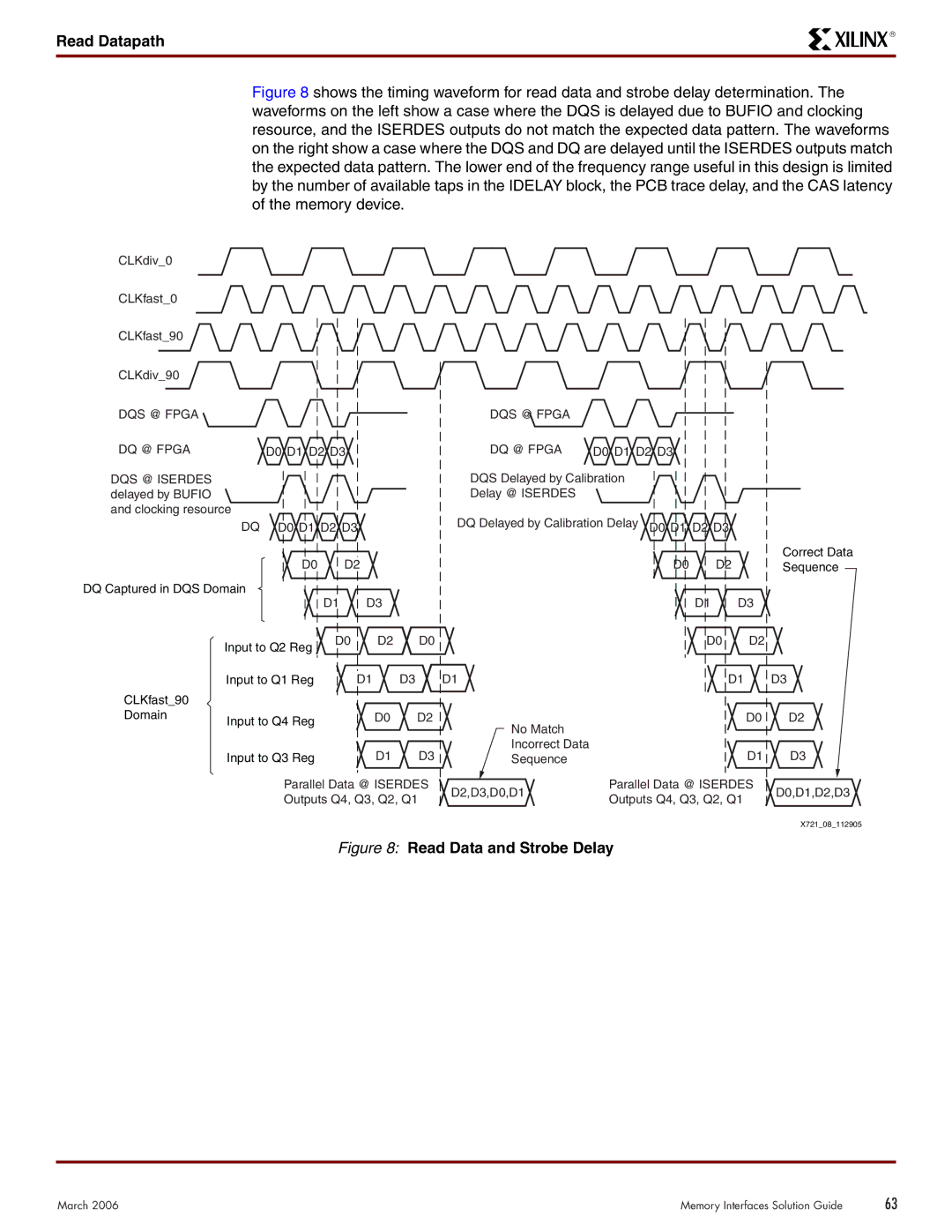
Figure 8 shows the timing waveform for read data and strobe delay determination. The waveforms on the left show a case where the DQS is delayed due to BUFIO and clocking resource, and the ISERDES outputs do not match the expected data pattern. The waveforms on the right show a case where the DQS and DQ are delayed until the ISERDES outputs match the expected data pattern. The lower end of the frequency range useful in this design is limited by the number of available taps in the IDELAY block, the PCB trace delay, and the CAS latency of the memory device.
CLKdiv_0
CLKfast_0
CLKfast_90
CLKdiv_90
DQS @ FPGA |
|
|
|
|
|
DQ @ FPGA |
| D0 D1 D2 D3 |
|
| |
DQS @ ISERDES |
|
|
|
|
|
delayed by BUFIO |
|
|
|
|
|
and clocking resource |
|
|
|
| |
| DQ | D0 D1 D2 D3 |
| ||
|
| D0 | D2 |
| |
DQ Captured in DQS Domain |
| D1 | D3 |
| |
|
|
|
| ||
| Input to Q2 Reg | D0 | D2 | D0 | |
|
|
|
| ||
| Input to Q1 Reg |
| D1 | D3 | |
CLKfast_90 |
|
|
|
|
|
Domain | Input to Q4 Reg |
| D0 | D2 | |
|
|
|
| ||
| Input to Q3 Reg |
| D1 | D3 | |
|
| Parallel Data @ ISERDES | |||
|
| Outputs Q4, Q3, Q2, Q1 | |||
DQS @ FPGA |
|
|
|
DQ @ FPGA | D0 D1 D2 D3 |
|
|
DQS Delayed by Calibration |
|
| |
Delay @ ISERDES |
|
|
|
DQ Delayed by Calibration Delay D0 D1 D2 D3 | |||
| D0 | D2 | |
|
| D1 | D3 |
|
| D0 | D2 |
D1 |
|
| D1 |
No Match |
|
| D0 |
|
|
| |
Incorrect Data |
|
| D1 |
Sequence |
|
| |
D2,D3,D0,D1 | Parallel Data @ ISERDES | |
Outputs Q4, Q3, Q2, Q1 | ||
|
Correct Data Sequence
D3
D2
D3
D0,D1,D2,D3
X721_08_112905
Figure 8: Read Data and Strobe Delay
March 2006 | Memory Interfaces Solution Guide | 63 |