Write Datapath
R
Controller to Write Datapath Interface
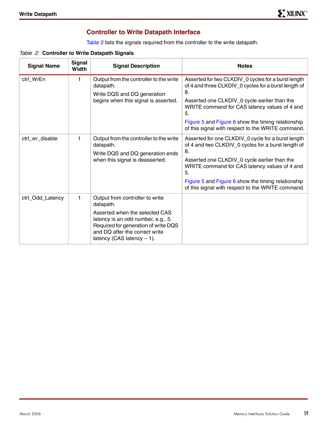
Table 2 lists the signals required from the controller to the write datapath.
Table 2: Controller to Write Datapath Signals
Signal Name | Signal | Signal Description | Notes | |
Width | ||||
|
|
| ||
|
|
|
| |
ctrl_WrEn | 1 | Output from the controller to the write | Asserted for two CLKDIV_0 cycles for a burst length | |
|
| datapath. | of 4 and three CLKDIV_0 cycles for a burst length of | |
|
| Write DQS and DQ generation | 8. | |
|
|
| ||
|
| begins when this signal is asserted. | Asserted one CLKDIV_0 cycle earlier than the | |
|
|
| WRITE command for CAS latency values of 4 and | |
|
|
| 5. | |
|
|
| Figure 5 and Figure 6 show the timing relationship | |
|
|
| of this signal with respect to the WRITE command. | |
|
|
|
| |
ctrl_wr_disable | 1 | Output from the controller to the write | Asserted for one CLKDIV_0 cycle for a burst length | |
|
| datapath. | of 4 and two CLKDIV_0 cycles for a burst length of | |
|
| Write DQS and DQ generation ends | 8. | |
|
|
| ||
|
| when this signal is deasserted. | Asserted one CLKDIV_0 cycle earlier than the | |
|
|
| WRITE command for CAS latency values of 4 and | |
|
|
| 5. | |
|
|
| Figure 5 and Figure 6 show the timing relationship | |
|
|
| of this signal with respect to the WRITE command. | |
|
|
|
| |
ctrl_Odd_Latency | 1 | Output from controller to write |
| |
|
| datapath. |
| |
|
| Asserted when the selected CAS |
| |
|
| latency is an odd number, e.g., 5. |
| |
|
| Required for generation of write DQS |
| |
|
| and DQ after the correct write |
| |
|
| latency (CAS latency – 1). |
| |
|
|
|
|
March 2006 | Memory Interfaces Solution Guide | 59 |