R
Write Datapath
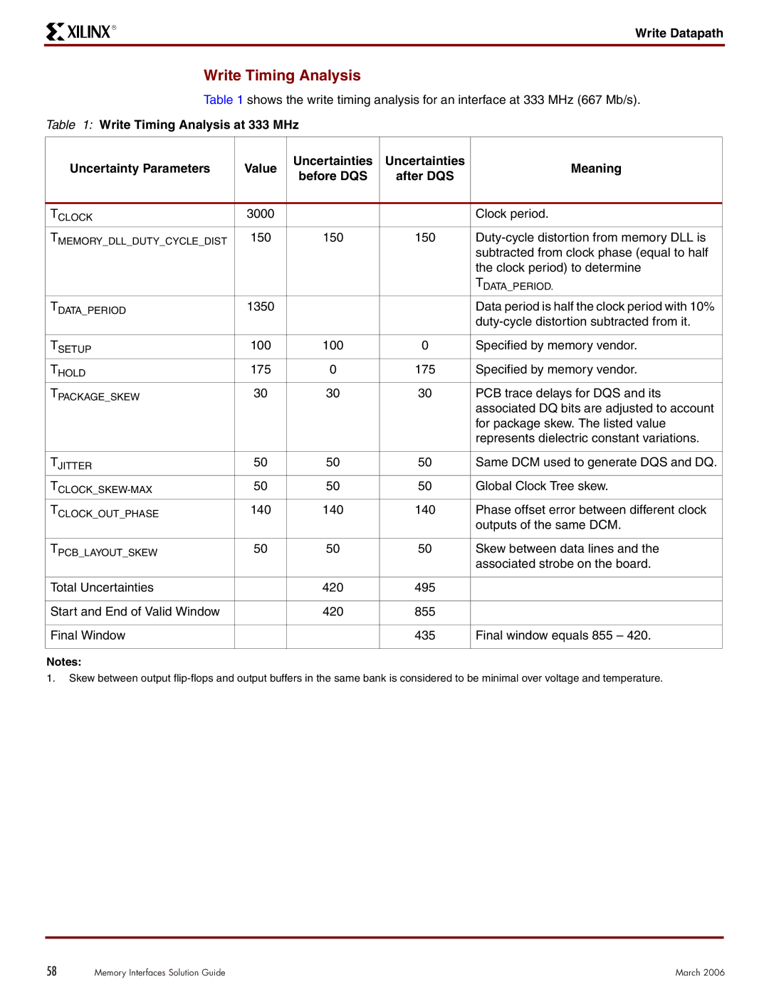
Write Timing Analysis
Table 1 shows the write timing analysis for an interface at 333 MHz (667 Mb/s).
Table 1: Write Timing Analysis at 333 MHz
Uncertainty Parameters | Value | Uncertainties | Uncertainties | Meaning | |
before DQS | after DQS | ||||
|
|
| |||
|
|
|
|
| |
TCLOCK | 3000 |
|
| Clock period. | |
TMEMORY_DLL_DUTY_CYCLE_DIST | 150 | 150 | 150 | ||
|
|
|
| subtracted from clock phase (equal to half | |
|
|
|
| the clock period) to determine | |
|
|
|
| TDATA_PERIOD. | |
TDATA_PERIOD | 1350 |
|
| Data period is half the clock period with 10% | |
|
|
|
| ||
|
|
|
|
| |
TSETUP | 100 | 100 | 0 | Specified by memory vendor. | |
THOLD | 175 | 0 | 175 | Specified by memory vendor. | |
TPACKAGE_SKEW | 30 | 30 | 30 | PCB trace delays for DQS and its | |
|
|
|
| associated DQ bits are adjusted to account | |
|
|
|
| for package skew. The listed value | |
|
|
|
| represents dielectric constant variations. | |
|
|
|
|
| |
TJITTER | 50 | 50 | 50 | Same DCM used to generate DQS and DQ. | |
50 | 50 | 50 | Global Clock Tree skew. | ||
TCLOCK_OUT_PHASE | 140 | 140 | 140 | Phase offset error between different clock | |
|
|
|
| outputs of the same DCM. | |
|
|
|
|
| |
TPCB_LAYOUT_SKEW | 50 | 50 | 50 | Skew between data lines and the | |
|
|
|
| associated strobe on the board. | |
|
|
|
|
| |
Total Uncertainties |
| 420 | 495 |
| |
|
|
|
|
| |
Start and End of Valid Window |
| 420 | 855 |
| |
|
|
|
|
| |
Final Window |
|
| 435 | Final window equals 855 – 420. | |
|
|
|
|
|
Notes:
1.Skew between output
58 | Memory Interfaces Solution Guide | March 2006 |