Contents
MZ-N10
ATRAC3 LP2/LP4
On power sources
Flexible Circuit Board Repairing
Polarity of the plug
Table of Contents
Section Servicing Notes
System requirements
Recorder Headphones/earphones with a remote control
Section General
Section Disassembly
Equipment can be removed using the following procedure
Bottom Panel Section, Jog Dial Section
Upper Panel Section
Main Board Section
MD Mechanism Deck MT-MZN10-181, Set Chassis
OP Service Assy ABX-1R
Gear SA, Gear SB
Holder Assy
Section Test Mode
Setting Method of Test Mode
Operation in Setting the Test Mode
Releasing the Test Mode
Configuration of Test Mode
Manual Mode
Transition method in manual mode
A n u a l
011 C 6 8 S 0
F F J 0
011 0 6 3 B 0
011 0 5 9 a 0
Reset the Error Display Code
L r O K ?
R r C L R
000 P * * R
000
000 FF
000 rFF
RMC OK
000 JOG+
000 JOG+OK
000 JOG
Reset
ResNV CC
ResOK?
021 Res
Power Supply Manual Adjustment
741 VC1 L
742 VC1 H
743 VC2 Lo
747 REG3L1
748 REG3L2
749 REG3 H
Vrec L
Vrec H
754 3.3upc
ChgV L
ChgV H
TP1907 REG3 TP1909 REG1
Power Supply Adjustment Auto Item Feed
Configuration of power supply adjustment auto item feed
Assy
ADJ OK
Laser
LrefPw @
HrefPw @
WrPwLo @
Configuration of overall adjustment mode
Adjusted values modifying procedure
881 ###S
882 ###S
Assy11
000 *** NG
CD OK
MO OK
MO overall adjustment items
Resume clear setting method
Resume
043 Res
ResClr
Rewriting the Patch Data at Replacement of Main Board
Preparation
Pre-check
Rewriting the patch data
MZ-N10
Confirmation of contents of the patch data rewrited
Removing the set
How to get the application NVWriter for NV values rewriting
Rewriting the NV values
Rewriting the NV values
MZ-N10
MZ-N10
MZ-N10
043
Remaining charging time Number of times of fully charging
Section Diagrams
Block Diagram
Waveforms
4Vp-p
Printed Wiring Board Main Board Side a Uses unleaded solder
Semiconductor Location
Main Board Side B Uses unleaded solder
Main Board
Schematic Diagrams Main Board 1/4 See page 38 for Waveforms
C513
270 ∝H
TC7SZ126AFE
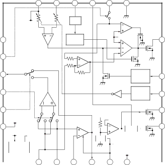
IC Block Diagrams
IC302 AN17020A-VB
IC502 XC62HR2202MR IC503 XC62HR2502MR
IC862 R2061K01-E2
IC951 SC901582EPR2
IC Pin Function Description
Sens
Fmck
Xskh
Xskl
Ffclr
Xcsnv
Joga
Jogb
Uosci
Uosco
SI3
SO3
Xras
XCS
DVSS0
DVSS1
FVDD0
FVSS0
Msak
Section Exploded Views
KNOB, Balance White . . . RED
Bottom Panel Section
US,CND,HK,KR,TW,E18,CH
Chassis Section
111 112 106 105 104 103
MD Mechanism Deck Section MT-MZN10-181
152 153 151
Main Electrical Parts List
Section
Main
CAP,CHIP Ceramic
Resistor
Switch
501 502
505
504 503
507
Memo
Revision History
Date Description of Revision
