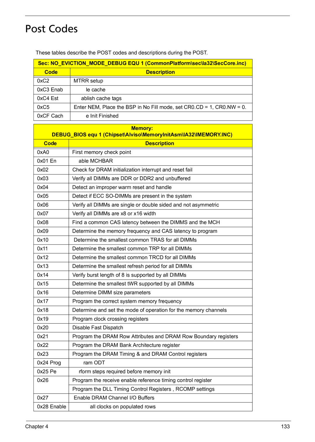
Post Codes
These tables describe the POST codes and descriptions during the POST.
Sec: NO_EVICTION_MODE_DEBUG EQU 1 (CommonPlatform\sec\Ia32\SecCore.inc)
Code | Description |
|
|
0xC2 | MTRR setup |
|
|
0xC3 Enab | le cache |
|
|
0xC4 Est | ablish cache tags |
|
|
0xC5 | Enter NEM, Place the BSP in No Fill mode, set CR0.CD = 1, CR0.NW = 0. |
|
|
0xCF Cach | e Init Finished |
|
|
Memory:
DEBUG_BIOS equ 1 (Chipset\Alviso\MemoryInitAsm\IA32\IMEMORY.INC)
Code | Description | |
|
|
|
0xA0 |
| First memory check point |
0x01 En | able MCHBAR | |
|
|
|
0x02 |
| Check for DRAM initialization interrupt and reset fail |
|
|
|
0x03 |
| Verify all DIMMs are DDR or DDR2 and unbuffered |
|
|
|
0x04 |
| Detect an improper warm reset and handle |
|
|
|
0x05 |
| Detect if ECC |
|
|
|
0x06 |
| Verify all DIMMs are single or double sided and not asymmetric |
|
|
|
0x07 |
| Verify all DIMMs are x8 or x16 width |
|
|
|
0x08 |
| Find a common CAS latency between the DIMMS and the MCH |
|
|
|
0x09 |
| Determine the memory frequency and CAS latency to program |
|
|
|
0x10 |
| Determine the smallest common TRAS for all DIMMs |
|
|
|
0x11 |
| Determine the smallest common TRP for all DIMMs |
|
|
|
0x12 |
| Determine the smallest common TRCD for all DIMMs |
|
|
|
0x13 |
| Determine the smallest refresh period for all DIMMs |
|
|
|
0x14 |
| Verify burst length of 8 is supported by all DIMMs |
|
|
|
0x15 |
| Determine the smallest tWR supported by all DIMMs |
|
|
|
0x16 |
| Determine DIMM size parameters |
|
|
|
0x17 |
| Program the correct system memory frequency |
|
|
|
0x18 |
| Determine and set the mode of operation for the memory channels |
|
|
|
0x19 |
| Program clock crossing registers |
|
|
|
0x20 |
| Disable Fast Dispatch |
|
|
|
0x21 |
| Program the DRAM Row Attributes and DRAM Row Boundary registers |
|
|
|
0x22 |
| Program the DRAM Bank Architecture register |
|
|
|
0x23 |
| Program the DRAM Timing & and DRAM Control registers |
|
| |
0x24 Prog | ram ODT | |
|
|
|
0x25 | Pe | rform steps required before memory init |
|
|
|
0x26 |
| Program the receive enable reference timing control register |
|
|
|
|
| Program the DLL Timing Control Registers , RCOMP settings |
|
|
|
0x27 |
| Enable DRAM Channel I/O Buffers |
|
|
|
0x28 | Enable | all clocks on populated rows |
|
|
|
Chapter 4 | 133 |