Page
Page
M740T/M740TU/M760T/M760TU
Trademarks
About this Manual
Important Safety Instructions
Instructions for Care and Operation
Power Safety
Battery Precautions
Preface
Contents
PCI-E LAN RTL8111C
Introduction
System Specifications
Feature Specification
System Specifications 1
Umts Modes
Optional Optical Drive Module Options
External Locator Top View with LCD Panel Open
Top View
Front Views
Right Side Views
Rear View
External Locator Left Side & Rear View
Left Side View
External Locator Bottom View
Bottom View
Mainboard Overview Top Key Parts
Mainboard Top Key Parts
Mainboard Overview Bottom Key Parts
Mainboard Bottom Key Parts
Mainboard Overview Top Connectors
Mainboard Top Connectors
Mainboard Overview Bottom Connectors
Mainboard Bottom Connectors
Introduction
Disassembly
Overview
Disassembly
Maintenance Precautions
Disassembly Steps
Disassembly
Removing the Battery
Battery Removal
HDD Assembly
Removing the Hard Disk Drive
Removing the Hard Disk Drive 2
For M760T/M760TU computers
M740T/M740TU
Removing the Optical CD/DVD Device
Optical Device Removal
Optical Device Removal cont’d
M760T/M760TU
Removing the System Memory RAM
RAM Module Removal
RAM Module Removal cont’d
Removing the Inverter Board
Inverter Board Removal
M740T/M740TU M760T/M760TU
Removing and Installing the Processor
Processor Removal
Unlock Lock
Processor Removal Cont’d
Processor Installation Procedure
Processor Installation
Removing the Wireless LAN Module
Wireless LAN Module Removal
Removing the Bluetooth Module
Bluetooth Module Removal
Removing the Keyboard
Keyboard Removal
Removing the Modem
Modem Removal
Modem Removal Cont’d M740T/M740TU e M760T/M760TU
M760T/M760TU 3434
Disassembly
Appendix a Part Lists
Part List Illustration Location
Part List Illustration Location
Top with Fingerprint M740T/M740TU
Top with Fingerprint M740T/M740TU
Top without Fingerprint M740T/M740TU
Bottom M740T
Bottom M740TU
Bottom M740TU
LCD M740T/M740TU
LCD M740T M740TU
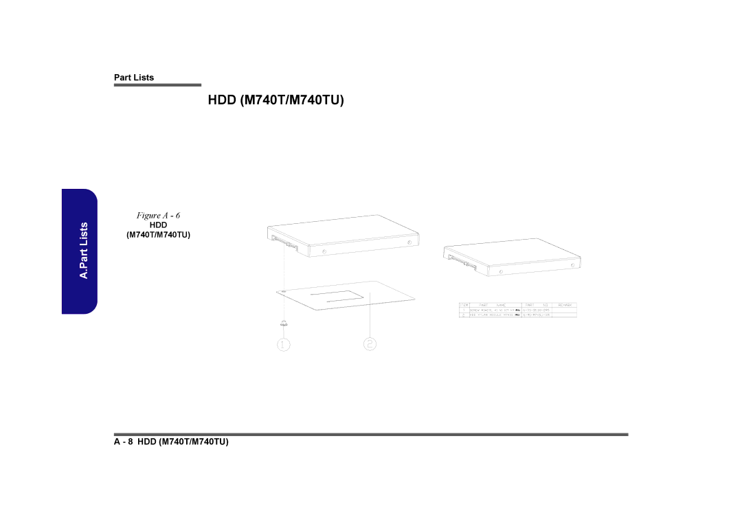
HDD M740T/M740TU
Combo M740T/M740TU
DVD-Dual Drive M740T/M740TU
DVD-Dual Drive M740T/M740TU
Top with Fingerprint M760T/M760TU
Top with Fingerprint M760T/M760TU
Top without Fingerprint M760T/M760TU
Bottom M760T
Bottom M760TU
Bottom M760TU
LCD M760T/M760TU
HDD M760T/M760TU
Combo M760T/M760TU
DVD-Dual Drive M760T/M760TU
DVD-Dual Drive M760T/M760TU
Appendix B Schematic Diagrams
Schematic Diagrams
System Block Diagram
Sheet 1 System Block Diagram
US B4
US B5
Clock Generator
Sheet 2 Clock Generator
Clock Generator
Layout note
Thermal Senser
Penryn Socket-P CPU 1/2
Sheet 3 Penryn Socket-P CPU 1/2
Penryn Socket-P CPU 2/2
Sheet 4 Penryn Socket-P CPU 2/2
I D 4 4 I D 5 4
5V S
Cantiga 1/7, Host
Sheet 5 Cantiga 1/7, Host
Cantiga 2/7, Graphics
Sheet 6
Graphics
MA X=
Cantiga 3/7
Sheet 7 of 51 Cantiga 3/7
Cantiga 4/7
Cantiga 5/7
Sheet 9 of 51 Cantiga 5/7
C D H P LL
Cantiga 6/7
Sheet 10 of 51 Cantiga 6/7
Cantiga 7/7
Sheet 11 of 51 Cantiga 7/7
Ddrii SO-DIMM
Sheet 12
D S P D
T E S T
B a 1 4
B B S 2 #
B B S 0 #
B B S 1 #
Panel, Inverter, CRT
Mode
VGA NB9M-1
Sheet 15 of 51 VGA NB9M-1
VGA NB9M-2
A D QM2
VGA NB9M-3
Sheet 17 of 51 VGA NB9M-3
VGA NB9M-4
Sheet 18 of 51 VGA NB9M-4
VGA NB9M-5
Sheet 19
VGA NB9M-6
Sheet 20 of 51 VGA NB9M-6
VGA NB9M-7
Sheet 21
ICH9M 1/4, Sata
Sheet 22
Sata HDD
Sata HDD & ODD LED
SPI*R = 0.1~0.5
ICH9M 2/4, PCI, USB
Place within
Power
Sheet 24 ICH9M 3/4
Sheet 25 ICH9M 4/4
C S a T a P L L
C G L a N P L L
C G LA N P L L
Mini Card
New Card, Mini Pcie
NEW Card
3G, Powergood
Sheet 27
3GEN
Uimvpp
USB, Fan, TP, FP, Multi CON
Conn
MI L
100 MIL
Card Reader
Sheet 29 Card Reader
Sata ODD, LED, Hotkey, LID SW
50m il
RTL8111C
PCI-E LAN RTL8111C
Sheet 31
Audio Codec ALC662
Sheet 32 Audio Codec ALC662
Codec
Beep
Audio AMP
Audio AMP
Sheet 33 of 51 Audio AMP
Fo r
KBCSPI*R = 0.1~0.5
? ? ?
Or IT 851 2C X/E
Power Plane
5VS, 3VS, 3.3VM, 1.05VS, VIN1
5VS
150mA
Power 3.3V/5V
Sheet 36 of 51 Power 3.3V/5V
TV C C
LD O5
Power 1.5VS/1.05VS
Sheet 37 of 51 Power 1.5VS/ 1.05VS
U T
OO D
Power 1.8V/0.9V
Sheet 38 Power 1.8V/0.9V
S a
TT E N
Power GPU/NVVDD
Sheet 39 Power GPU/NVVDD
Vgfxcore
PU2 R a MP
AC-IN, Charger
Dcjack
CT L
CH G E N
Sheet 41
Close to IMVP6
GND P a D
Nvvdd
Sheet 42
Sheet 43
External ODD Board for M76
Sheet 44 External ODD Board for M76
Click & Finger Board for M76
Sheet 45 Click Finger Board For M76
Ns tuf f 10mil
30 K0
Multi Function Board
Sheet 46 Multi Function Board
Multi I/O Conn
MDC
Audio Board
Sheet 47
Audio Board
50 mil
Finger Sensor Board for M76
Sheet 48 of 51 Finger Sensor Board for M76
SMB TN #
Power Switch Board for M74
Sheet 49 of 51 Power Switch Board for M74
FingerPrint Board for M74
Sheet 50 FingerPrint Board For M74
SH B TN #
Power Switch Board for M76
Sheet 51 of 51 Power Switch Board for M76