Connect Tech
Connector Pinouts
Refer to
Note: P1 must be connected to a
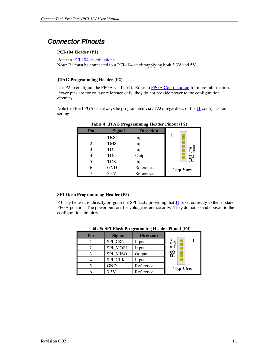
JTAG Programming Header (P2)
Use P2 to configure the FPGA via JTAG. Refer to FPGA Configuration for more information. Power pins are for voltage reference only; they do not provide power to the configuration circuitry.
Note that the FPGA can always be programmed via JTAG, regardless of the J1 configuration setting.
Table 4: JTAG Programming Header Pinout (P2)
Pin
Signal
Direction
1 | TRST | Input | 1 |
|
|
|
|
|
|
|
| ||||
|
|
|
|
| |||
2 | TMS | Input |
|
|
|
| JTAG Header |
3 | TDI | Input |
|
|
|
| |
|
|
|
|
| |||
4 | TDO | Output |
|
|
|
| P2 |
5 | TCK | Input |
|
|
|
| |
|
|
|
|
| |||
6 | GND | Reference | Top View | ||||
|
|
| |||||
7
3.3V
Reference
SPI Flash Programming Header (P3)
P3 may be used to directly program the SPI flash, providing that J1 is set correctly to the
Table 5: SPI Flash Programming Header Pinout (P3)
Pin |
|
| Signal |
| Direction | FlashSPI |
|
|
|
|
1 |
|
| SPI_CSN |
| Input | Header |
|
| 1 | |
|
|
|
|
|
|
| ||||
2 |
|
| SPI_MOSI |
| Input | P3 |
|
|
| |
3 |
|
| SPI_MISO |
| Output |
|
|
| ||
|
|
|
|
|
|
|
| |||
4 |
|
| SPI_CLK |
| Input |
|
|
|
|
|
5 |
|
| GND |
| Reference |
|
|
|
|
|
|
|
|
| Top View | ||||||
6 |
|
| 3.3V |
| Reference |
| ||||
|
|
|
|
|
|
|
| |||
Revision 0.02 | 11 |