PRELIMINARY | CY14B108L, CY14B108N |
|
8 Mbit (1024K x 8/512K x 16) nvSRAM
Features
■20 ns, 25 ns, and 45 ns Access Times
■Internally organized as 1024K x 8 (CY14B108L) or 512K x 16 (CY14B108N)
■Hands off Automatic STORE on power down with only a small Capacitor
■STORE to QuantumTrap® nonvolatile elements initiated by Software, device pin, or AutoStore® on power down
■RECALL to SRAM initiated by Software or power up
■Infinite Read, Write, and RECALL Cycles
■200,000 STORE cycles to QuantumTrap
■20 year data retention
■Single 3V +20%,
■Commercial and Industrial Temperatures
■
■
Functional Description
The Cypress CY14B108L/CY14B108N is a fast static RAM, with a nonvolatile element in each memory cell. The memory is organized as 1024 Kbytes of 8 bits each or 512K words of 16 bits each. The embedded nonvolatile elements incorporate QuantumTrap technology, producing the world’s most reliable nonvolatile memory. The SRAM provides infinite read and write cycles, while independent nonvolatile data resides in the highly reliable QuantumTrap cell. Data transfers from the SRAM to the nonvolatile elements (the STORE operation) takes place automatically at power down. On power up, data is restored to the SRAM (the RECALL operation) from the nonvolatile memory. Both the STORE and RECALL operations are also available under software control.
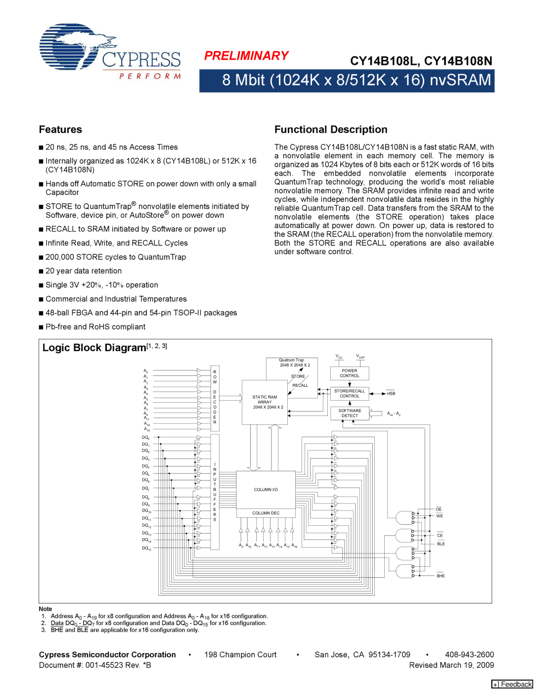
Logic Block Diagram[1, 2, 3]
|
|
| Quatrum Trap | VCC | VCAP |
| ||
|
|
|
|
|
| |||
A0 |
|
| 2048 X 2048 X 2 |
|
|
| ||
R |
|
|
|
| POWER |
| ||
A1 | O |
|
|
| STORE | CONTROL |
| |
A2 | W |
|
|
| RECALL |
|
|
|
A3 |
|
|
|
|
|
|
| |
D |
|
|
|
| STORE/RECALL |
| ||
A4 |
|
|
|
| HSB | |||
A5 | E |
| STATIC RAM |
|
| CONTROL |
| |
A6 | C |
| ARRAY |
|
|
|
|
|
A7 | O |
| 2048 X 2048 X 2 |
|
| SOFTWARE |
| |
D |
|
|
|
|
| |||
A8 |
|
|
|
| DETECT | A14 - A2 | ||
E |
|
|
|
| ||||
A17 |
|
|
|
|
|
|
| |
A18 | R |
|
|
|
|
|
|
|
A19 |
|
|
|
|
|
|
|
|
DQ0 |
|
|
|
|
|
|
|
|
DQ1 |
|
|
|
|
|
|
|
|
DQ2 |
|
|
|
|
|
|
|
|
DQ3 | I |
|
|
|
|
|
|
|
DQ4 |
|
|
|
|
|
|
| |
N |
|
|
|
|
|
|
| |
DQ5 |
|
|
|
|
|
|
| |
P |
|
|
|
|
|
|
| |
DQ6 | U |
|
|
|
|
|
|
|
DQ7 | T |
|
|
|
|
|
|
|
B |
| COLUMN I/O |
|
|
|
|
| |
DQ8 | U |
|
|
|
|
|
|
|
F |
|
|
|
|
|
|
| |
DQ9 | F |
|
|
|
|
|
|
|
DQ10 | E |
| COLUMN DEC |
|
|
|
|
|
R |
|
|
|
|
|
| ||
DQ11 |
|
|
|
|
|
|
| |
S |
|
|
|
|
|
|
| |
DQ12 |
|
|
|
|
|
|
|
|
DQ13 |
|
|
|
|
|
|
|
|
DQ14 | A9 | A10 | A11 A12 A13 A14 | A15 | A16 |
|
|
|
DQ15 |
|
|
| |||||
|
|
|
|
|
|
|
| |
OE WE
CE
BLE
BHE
Note |
|
|
|
|
|
| ||
1. | Address A0 - A19 for x8 configuration and Address A0 | - A18 for x16 configuration. |
|
|
|
| ||
2. | Data DQ0 | - DQ7 for x8 configuration and Data DQ0 | - DQ15 for x16 configuration. |
|
|
|
| |
3. | BHE and | BLE are applicable for x16 configuration only. |
|
|
|
| ||
Cypress Semiconductor Corporation | • | 198 Champion Court | • | San Jose, CA | • | |||
Document #: |
|
|
| Revised March 19, 2009 | ||||
[+] Feedback